- 您现在的位置:买卖IC网 > PDF目录12027 > ADUC7021BCPZ62 (Analog Devices Inc)IC MCU FLSH 62K ANLG I/O 40LFCSP PDF资料下载
参数资料
| 型号: | ADUC7021BCPZ62 |
| 厂商: | Analog Devices Inc |
| 文件页数: | 46/104页 |
| 文件大小: | 0K |
| 描述: | IC MCU FLSH 62K ANLG I/O 40LFCSP |
| 产品培训模块: | ARM7 Applications & Tools Process Control |
| 标准包装: | 1 |
| 系列: | MicroConverter® ADuC7xxx |
| 核心处理器: | ARM7 |
| 芯体尺寸: | 16/32-位 |
| 速度: | 44MHz |
| 连通性: | EBI/EMI,I²C,SPI,UART/USART |
| 外围设备: | PLA,PWM,PSM,温度传感器,WDT |
| 输入/输出数: | 13 |
| 程序存储器容量: | 64KB(32K x 16) |
| 程序存储器类型: | 闪存 |
| RAM 容量: | 2K x 32 |
| 电压 - 电源 (Vcc/Vdd): | 2.7 V ~ 3.6 V |
| 数据转换器: | A/D 8x12b,D/A 2x12b |
| 振荡器型: | 内部 |
| 工作温度: | -40°C ~ 125°C |
| 封装/外壳: | 40-VFQFN 裸露焊盘,CSP |
| 包装: | 托盘 |
第1页第2页第3页第4页第5页第6页第7页第8页第9页第10页第11页第12页第13页第14页第15页第16页第17页第18页第19页第20页第21页第22页第23页第24页第25页第26页第27页第28页第29页第30页第31页第32页第33页第34页第35页第36页第37页第38页第39页第40页第41页第42页第43页第44页第45页当前第46页第47页第48页第49页第50页第51页第52页第53页第54页第55页第56页第57页第58页第59页第60页第61页第62页第63页第64页第65页第66页第67页第68页第69页第70页第71页第72页第73页第74页第75页第76页第77页第78页第79页第80页第81页第82页第83页第84页第85页第86页第87页第88页第89页第90页第91页第92页第93页第94页第95页第96页第97页第98页第99页第100页第101页第102页第103页第104页
ADuC7019/20/21/22/24/25/26/27/28/29
Data Sheet
Rev. F | Page 46 of 104
TYPICAL OPERATION
Once configured via the ADC control and channel selection
registers, the ADC converts the analog input and provides a
12-bit result in the ADC data register.
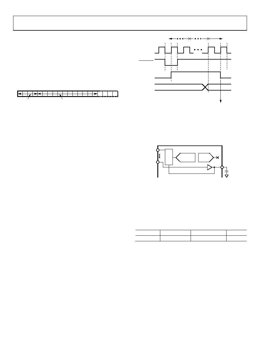
The top four bits are the sign bits. The 12-bit result is placed
from Bit 16 to Bit 27, as shown in Figure 51. Again, it should be
noted that, in fully differential mode, the result is represented in
twos complement format. In pseudo differential and single-
ended modes, the result is represented in straight binary format.
04
95
5-
01
4
SIGN BITS
12-BIT ADC RESULT
31
27
16 15
0
Figure 51. ADC Result Format
The same format is used in DACxDAT, simplifying the software.
Current Consumption
The ADC in standby mode, that is, powered up but not
converting, typically consumes 640 μA. The internal reference
adds 140 μA. During conversion, the extra current is 0.3 μA
multiplied by the sampling frequency (in kilohertz (kHz)).
Figure 43 shows the current consumption vs. the sampling
frequency of the ADC.
Timing
Figure 52 gives details of the ADC timing. Users control the
ADC clock speed and the number of acquisition clocks in the
ADCCON MMR. By default, the acquisition time is eight clocks
and the clock divider is 2. The number of extra clocks (such as
bit trial or write) is set to 19, which gives a sampling rate of
774 kSPS. For conversion on the temperature sensor, the ADC
acquisition time is automatically set to 16 clocks, and the ADC
clock divider is set to 32. When using multiple channels,
including the temperature sensor, the timing settings revert to
the user-defined settings after reading the temperature sensor
channel.
0
495
5-
015
ADC CLOCK
ACQ
BIT TRIAL
DATA
ADCSTA = 0
ADCSTA = 1
ADC INTERRUPT
WRITE
CONVSTART
ADCBUSY
ADCDAT
Figure 52. ADC Timing
ADuC7019
The ADuC7019 is identical to the ADuC7020 except for one
buffered ADC channel, ADC3, and it has only three DACs. The
output buffer of the fourth DAC is internally connected to the
ADC3 channel as shown in Figure 53.
04
95
5-
016
1MSPS
12-BIT ADC
12-BIT
DAC
MUX
ADC3
ADC15
DAC3
ADuC7019
Figure 53. ADC3 Buffered Input
Note that the DAC3 output pin must be connected to a 10 nF
capacitor to AGND. This channel should be used to measure dc
voltages only. ADC calibration may be necessary on this channel.
MMRS INTERFACE
The ADC is controlled and configured via the eight MMRs
described in this section.
Table 17. ADCCON Register
Name
Address
Default Value
Access
ADCCON
0xFFFF0500
0x0600
R/W
ADCCON is an ADC control register that allows the programmer
to enable the ADC peripheral, select the mode of operation of
the ADC (in single-ended mode, pseudo differential mode, or
fully differential mode), and select the conversion type. This
MMR is described in Table 18.
相关PDF资料 |
PDF描述 |
|---|---|
| VI-B2M-IY-F3 | CONVERTER MOD DC/DC 10V 50W |
| MUSB-2A111-024BP | DUST COVER FOR MUSB TYPE A BLACK |
| VI-B2M-IY-F2 | CONVERTER MOD DC/DC 10V 50W |
| AT89C51AC3-S3SUM | IC 8051 MCU 64K FLASH 52-PLCC |
| VI-B2M-IY-F1 | CONVERTER MOD DC/DC 10V 50W |
相关代理商/技术参数 |
参数描述 |
|---|---|
| ADUC7021BCPZ62I | 功能描述:IC MCU FLSH 62K ANLG I/O 40LFCSP RoHS:是 类别:集成电路 (IC) >> 嵌入式 - 微控制器, 系列:MicroConverter® ADuC7xxx 产品培训模块:MCU Product Line Introduction XMEGA Introduction AVR XMEGA USB Connectivity 标准包装:90 系列:AVR® XMEGA 核心处理器:AVR 芯体尺寸:8/16-位 速度:32MHz 连通性:I²C,IrDA,SPI,UART/USART 外围设备:欠压检测/复位,DMA,POR,PWM,WDT 输入/输出数:50 程序存储器容量:192KB(96K x 16) 程序存储器类型:闪存 EEPROM 大小:4K x 8 RAM 容量:16K x 8 电压 - 电源 (Vcc/Vdd):1.6 V ~ 3.6 V 数据转换器:A/D 16x12b; D/A 2x12b 振荡器型:内部 工作温度:-40°C ~ 85°C 封装/外壳:64-TQFP 包装:托盘 配用:ATSTK600-RC14-ND - STK600 SOCKET/ADAPTER 64TQFPATSTK600-TQFP64-ND - STK600 SOCKET/ADAPTER 64-TQFPATAVRONEKIT-ND - KIT AVR/AVR32 DEBUGGER/PROGRMMRATAVRISP2-ND - PROGRAMMER AVR IN SYSTEM |
| ADUC7021BCPZ62I-RL | 功能描述:IC MCU 12BIT 1MSPS I2C 40-LFCSP RoHS:是 类别:集成电路 (IC) >> 嵌入式 - 微控制器, 系列:MicroConverter® ADuC7xxx 标准包装:38 系列:Encore!® XP® 核心处理器:eZ8 芯体尺寸:8-位 速度:5MHz 连通性:IrDA,UART/USART 外围设备:欠压检测/复位,LED,POR,PWM,WDT 输入/输出数:16 程序存储器容量:4KB(4K x 8) 程序存储器类型:闪存 EEPROM 大小:- RAM 容量:1K x 8 电压 - 电源 (Vcc/Vdd):2.7 V ~ 3.6 V 数据转换器:- 振荡器型:内部 工作温度:-40°C ~ 105°C 封装/外壳:20-SOIC(0.295",7.50mm 宽) 包装:管件 其它名称:269-4116Z8F0413SH005EG-ND |
| ADUC7021BCPZ62IRL7 | 制造商:Analog Devices 功能描述:MCU 16-bit/32-bit ADuC7xxx ARM7TDMI RISC 62KB Flash 3.3V 40-Pin LFCSP EP T/R |
| ADUC7021BCPZ62-RL | 功能描述:IC MCU 12BIT 1MSPS UART 40-LFCSP RoHS:是 类别:集成电路 (IC) >> 嵌入式 - 微控制器, 系列:MicroConverter® ADuC7xxx 标准包装:38 系列:Encore!® XP® 核心处理器:eZ8 芯体尺寸:8-位 速度:5MHz 连通性:IrDA,UART/USART 外围设备:欠压检测/复位,LED,POR,PWM,WDT 输入/输出数:16 程序存储器容量:4KB(4K x 8) 程序存储器类型:闪存 EEPROM 大小:- RAM 容量:1K x 8 电压 - 电源 (Vcc/Vdd):2.7 V ~ 3.6 V 数据转换器:- 振荡器型:内部 工作温度:-40°C ~ 105°C 封装/外壳:20-SOIC(0.295",7.50mm 宽) 包装:管件 其它名称:269-4116Z8F0413SH005EG-ND |
| ADUC7021BCPZ62-RL7 | 功能描述:IC MCU 12BIT 1MSPS UART 40-LFCSP RoHS:是 类别:集成电路 (IC) >> 嵌入式 - 微控制器, 系列:MicroConverter® ADuC7xxx 标准包装:38 系列:Encore!® XP® 核心处理器:eZ8 芯体尺寸:8-位 速度:5MHz 连通性:IrDA,UART/USART 外围设备:欠压检测/复位,LED,POR,PWM,WDT 输入/输出数:16 程序存储器容量:4KB(4K x 8) 程序存储器类型:闪存 EEPROM 大小:- RAM 容量:1K x 8 电压 - 电源 (Vcc/Vdd):2.7 V ~ 3.6 V 数据转换器:- 振荡器型:内部 工作温度:-40°C ~ 105°C 封装/外壳:20-SOIC(0.295",7.50mm 宽) 包装:管件 其它名称:269-4116Z8F0413SH005EG-ND |
发布紧急采购,3分钟左右您将得到回复。