- 您现在的位置:买卖IC网 > PDF目录12027 > ADUC7021BCPZ62 (Analog Devices Inc)IC MCU FLSH 62K ANLG I/O 40LFCSP PDF资料下载
参数资料
| 型号: | ADUC7021BCPZ62 |
| 厂商: | Analog Devices Inc |
| 文件页数: | 80/104页 |
| 文件大小: | 0K |
| 描述: | IC MCU FLSH 62K ANLG I/O 40LFCSP |
| 产品培训模块: | ARM7 Applications & Tools Process Control |
| 标准包装: | 1 |
| 系列: | MicroConverter® ADuC7xxx |
| 核心处理器: | ARM7 |
| 芯体尺寸: | 16/32-位 |
| 速度: | 44MHz |
| 连通性: | EBI/EMI,I²C,SPI,UART/USART |
| 外围设备: | PLA,PWM,PSM,温度传感器,WDT |
| 输入/输出数: | 13 |
| 程序存储器容量: | 64KB(32K x 16) |
| 程序存储器类型: | 闪存 |
| RAM 容量: | 2K x 32 |
| 电压 - 电源 (Vcc/Vdd): | 2.7 V ~ 3.6 V |
| 数据转换器: | A/D 8x12b,D/A 2x12b |
| 振荡器型: | 内部 |
| 工作温度: | -40°C ~ 125°C |
| 封装/外壳: | 40-VFQFN 裸露焊盘,CSP |
| 包装: | 托盘 |
第1页第2页第3页第4页第5页第6页第7页第8页第9页第10页第11页第12页第13页第14页第15页第16页第17页第18页第19页第20页第21页第22页第23页第24页第25页第26页第27页第28页第29页第30页第31页第32页第33页第34页第35页第36页第37页第38页第39页第40页第41页第42页第43页第44页第45页第46页第47页第48页第49页第50页第51页第52页第53页第54页第55页第56页第57页第58页第59页第60页第61页第62页第63页第64页第65页第66页第67页第68页第69页第70页第71页第72页第73页第74页第75页第76页第77页第78页第79页当前第80页第81页第82页第83页第84页第85页第86页第87页第88页第89页第90页第91页第92页第93页第94页第95页第96页第97页第98页第99页第100页第101页第102页第103页第104页
Data Sheet
ADuC7019/20/21/22/24/25/26/27/28/29
Rev. F | Page 77 of 104
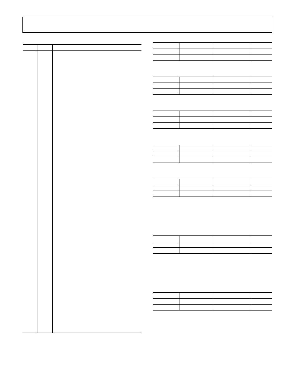
Table 129. I2C0SSTA MMR Bit Descriptions
Bit
Value
Description
31:15
Reserved. These bits should be written as 0.
14
Start decode bit. Set by hardware if the device
receives a valid start plus matching address.
Cleared by an I2C stop condition or an I2C
general call reset.
13
Repeated start decode bit. Set by hardware
if the device receives a valid repeated start and
matching address. Cleared by an I2C stop condi-
tion, a read of the I2CSSTA register, or an I2C
general call reset.
12:11
ID decode bits.
00
Received Address Matched ID Register 0.
01
Received Address Matched ID Register 1.
10
Received Address Matched ID Register 2.
11
Received Address Matched ID Register 3.
10
Stop after start and matching address interrupt.
Set by hardware if the slave device receives an
I2C stop condition after a previous I2C start
condition and matching address. Cleared by a
read of the I2C0SSTA register.
9:8
General call ID.
00
No general call.
01
General call reset and program address.
10
General call program address.
11
General call matching alternative ID.
7
General call interrupt. Set if the slave device
receives a general call of any type. Cleared by
setting Bit 8 of the I2CxCFG register. If it is a
general call reset, all registers are at their
default values. If it is a hardware general call,
the Rx FIFO holds the second byte of the
general call. This is similar to the I2C0ALT
register (unless it is a general call to reprogram
the device address). For more details, see the I2C
bus specification, Version 2.1, January 2000.
6
Slave busy. Set automatically if the slave is busy.
Cleared automatically.
5
No ACK. Set if master asking for data and no
data is available. Cleared automatically by
reading the I2C0SSTA register.
4
Slave receive FIFO overflow. Set automatically if
the slave receive FIFO is overflowing. Cleared
automatically by reading the I2C0SSTA register.
3
Slave receive IRQ. Set after receiving data.
Cleared automatically by reading the I2C0SRX
register or flushing the FIFO.
2
Slave transmit IRQ. Set at the end of a trans-
mission. Cleared automatically by writing to the
I2C0STX register.
1
Slave transmit FIFO underflow. Set automatically if
the slave transmit FIFO is underflowing. Cleared
automatically by writing to the I2C0SSTA register.
0
Slave transmit FIFO not full. Set automatically if
the slave transmit FIFO is not full. Cleared auto-
matically by writing twice to the I2C0STX register.
Table 130. I2CxSRX Registers
Name
Address
Default Value
Access
I2C0SRX
0xFFFF0808
0x00
R
I2C1SRX
0xFFFF0908
0x00
R
I2CxSRX are receive registers for the slave channel.
Table 131. I2CxSTX Registers
Name
Address
Default Value
Access
I2C0STX
0xFFFF080C
0x00
W
I2C1STX
0xFFFF090C
0x00
W
I2CxSTX are transmit registers for the slave channel.
Table 132. I2CxMRX Registers
Name
Address
Default Value
Access
I2C0MRX
0xFFFF0810
0x00
R
I2C1MRX
0xFFFF0910
0x00
R
I2CxMRX are receive registers for the master channel.
Table 133. I2CxMTX Registers
Name
Address
Default Value
Access
I2C0MTX
0xFFFF0814
0x00
W
I2C1MTX
0xFFFF0914
0x00
W
I2CxMTX are transmit registers for the master channel.
Table 134. I2CxCNT Registers
Name
Address
Default Value
Access
I2C0CNT
0xFFFF0818
0x00
R/W
I2C1CNT
0xFFFF0918
0x00
R/W
I2CxCNT are 3-bit, master receive, data count registers. If a master
read transfer sequence is initiated, the I2CxCNT registers denote
the number of bytes (1) to be read from the slave device. By
default, this counter is 0, which corresponds to the one byte
expected.
Table 135. I2CxADR Registers
Name
Address
Default Value
Access
I2C0ADR
0xFFFF081C
0x00
R/W
I2C1ADR
0xFFFF091C
0x00
R/W
I2CxADR are master address byte registers. The I2CxADR
value is the device address that the master wants to commun-
icate with. It automatically transmits at the start of a master
transfer sequence if there is no valid data in the I2CxMTX
register when the master enable bit is set.
Table 136. I2CxBYTE Registers
Name
Address
Default Value
Access
I2C0BYTE
0xFFFF0824
0x00
R/W
I2C1BYTE
0xFFFF0924
0x00
R/W
I2CxBYTE are broadcast byte registers. Data written to these
registers does not go through the TxFIFO. This data is transmitted
at the start of a transfer sequence before the address. After the
byte is transmitted and acknowledged, the I2C expects another
byte written in I2CxBYTE or an address written to the address
register.
相关PDF资料 |
PDF描述 |
|---|---|
| VI-B2M-IY-F3 | CONVERTER MOD DC/DC 10V 50W |
| MUSB-2A111-024BP | DUST COVER FOR MUSB TYPE A BLACK |
| VI-B2M-IY-F2 | CONVERTER MOD DC/DC 10V 50W |
| AT89C51AC3-S3SUM | IC 8051 MCU 64K FLASH 52-PLCC |
| VI-B2M-IY-F1 | CONVERTER MOD DC/DC 10V 50W |
相关代理商/技术参数 |
参数描述 |
|---|---|
| ADUC7021BCPZ62I | 功能描述:IC MCU FLSH 62K ANLG I/O 40LFCSP RoHS:是 类别:集成电路 (IC) >> 嵌入式 - 微控制器, 系列:MicroConverter® ADuC7xxx 产品培训模块:MCU Product Line Introduction XMEGA Introduction AVR XMEGA USB Connectivity 标准包装:90 系列:AVR® XMEGA 核心处理器:AVR 芯体尺寸:8/16-位 速度:32MHz 连通性:I²C,IrDA,SPI,UART/USART 外围设备:欠压检测/复位,DMA,POR,PWM,WDT 输入/输出数:50 程序存储器容量:192KB(96K x 16) 程序存储器类型:闪存 EEPROM 大小:4K x 8 RAM 容量:16K x 8 电压 - 电源 (Vcc/Vdd):1.6 V ~ 3.6 V 数据转换器:A/D 16x12b; D/A 2x12b 振荡器型:内部 工作温度:-40°C ~ 85°C 封装/外壳:64-TQFP 包装:托盘 配用:ATSTK600-RC14-ND - STK600 SOCKET/ADAPTER 64TQFPATSTK600-TQFP64-ND - STK600 SOCKET/ADAPTER 64-TQFPATAVRONEKIT-ND - KIT AVR/AVR32 DEBUGGER/PROGRMMRATAVRISP2-ND - PROGRAMMER AVR IN SYSTEM |
| ADUC7021BCPZ62I-RL | 功能描述:IC MCU 12BIT 1MSPS I2C 40-LFCSP RoHS:是 类别:集成电路 (IC) >> 嵌入式 - 微控制器, 系列:MicroConverter® ADuC7xxx 标准包装:38 系列:Encore!® XP® 核心处理器:eZ8 芯体尺寸:8-位 速度:5MHz 连通性:IrDA,UART/USART 外围设备:欠压检测/复位,LED,POR,PWM,WDT 输入/输出数:16 程序存储器容量:4KB(4K x 8) 程序存储器类型:闪存 EEPROM 大小:- RAM 容量:1K x 8 电压 - 电源 (Vcc/Vdd):2.7 V ~ 3.6 V 数据转换器:- 振荡器型:内部 工作温度:-40°C ~ 105°C 封装/外壳:20-SOIC(0.295",7.50mm 宽) 包装:管件 其它名称:269-4116Z8F0413SH005EG-ND |
| ADUC7021BCPZ62IRL7 | 制造商:Analog Devices 功能描述:MCU 16-bit/32-bit ADuC7xxx ARM7TDMI RISC 62KB Flash 3.3V 40-Pin LFCSP EP T/R |
| ADUC7021BCPZ62-RL | 功能描述:IC MCU 12BIT 1MSPS UART 40-LFCSP RoHS:是 类别:集成电路 (IC) >> 嵌入式 - 微控制器, 系列:MicroConverter® ADuC7xxx 标准包装:38 系列:Encore!® XP® 核心处理器:eZ8 芯体尺寸:8-位 速度:5MHz 连通性:IrDA,UART/USART 外围设备:欠压检测/复位,LED,POR,PWM,WDT 输入/输出数:16 程序存储器容量:4KB(4K x 8) 程序存储器类型:闪存 EEPROM 大小:- RAM 容量:1K x 8 电压 - 电源 (Vcc/Vdd):2.7 V ~ 3.6 V 数据转换器:- 振荡器型:内部 工作温度:-40°C ~ 105°C 封装/外壳:20-SOIC(0.295",7.50mm 宽) 包装:管件 其它名称:269-4116Z8F0413SH005EG-ND |
| ADUC7021BCPZ62-RL7 | 功能描述:IC MCU 12BIT 1MSPS UART 40-LFCSP RoHS:是 类别:集成电路 (IC) >> 嵌入式 - 微控制器, 系列:MicroConverter® ADuC7xxx 标准包装:38 系列:Encore!® XP® 核心处理器:eZ8 芯体尺寸:8-位 速度:5MHz 连通性:IrDA,UART/USART 外围设备:欠压检测/复位,LED,POR,PWM,WDT 输入/输出数:16 程序存储器容量:4KB(4K x 8) 程序存储器类型:闪存 EEPROM 大小:- RAM 容量:1K x 8 电压 - 电源 (Vcc/Vdd):2.7 V ~ 3.6 V 数据转换器:- 振荡器型:内部 工作温度:-40°C ~ 105°C 封装/外壳:20-SOIC(0.295",7.50mm 宽) 包装:管件 其它名称:269-4116Z8F0413SH005EG-ND |
发布紧急采购,3分钟左右您将得到回复。