- 您现在的位置:买卖IC网 > PDF目录12027 > ADUC7021BCPZ62 (Analog Devices Inc)IC MCU FLSH 62K ANLG I/O 40LFCSP PDF资料下载
参数资料
| 型号: | ADUC7021BCPZ62 |
| 厂商: | Analog Devices Inc |
| 文件页数: | 65/104页 |
| 文件大小: | 0K |
| 描述: | IC MCU FLSH 62K ANLG I/O 40LFCSP |
| 产品培训模块: | ARM7 Applications & Tools Process Control |
| 标准包装: | 1 |
| 系列: | MicroConverter® ADuC7xxx |
| 核心处理器: | ARM7 |
| 芯体尺寸: | 16/32-位 |
| 速度: | 44MHz |
| 连通性: | EBI/EMI,I²C,SPI,UART/USART |
| 外围设备: | PLA,PWM,PSM,温度传感器,WDT |
| 输入/输出数: | 13 |
| 程序存储器容量: | 64KB(32K x 16) |
| 程序存储器类型: | 闪存 |
| RAM 容量: | 2K x 32 |
| 电压 - 电源 (Vcc/Vdd): | 2.7 V ~ 3.6 V |
| 数据转换器: | A/D 8x12b,D/A 2x12b |
| 振荡器型: | 内部 |
| 工作温度: | -40°C ~ 125°C |
| 封装/外壳: | 40-VFQFN 裸露焊盘,CSP |
| 包装: | 托盘 |
第1页第2页第3页第4页第5页第6页第7页第8页第9页第10页第11页第12页第13页第14页第15页第16页第17页第18页第19页第20页第21页第22页第23页第24页第25页第26页第27页第28页第29页第30页第31页第32页第33页第34页第35页第36页第37页第38页第39页第40页第41页第42页第43页第44页第45页第46页第47页第48页第49页第50页第51页第52页第53页第54页第55页第56页第57页第58页第59页第60页第61页第62页第63页第64页当前第65页第66页第67页第68页第69页第70页第71页第72页第73页第74页第75页第76页第77页第78页第79页第80页第81页第82页第83页第84页第85页第86页第87页第88页第89页第90页第91页第92页第93页第94页第95页第96页第97页第98页第99页第100页第101页第102页第103页第104页
Data Sheet
ADuC7019/20/21/22/24/25/26/27/28/29
Rev. F | Page 63 of 104
The PWMDAT1 register is a 10-bit register with a maximum
value of 0x3FF (= 1023), which corresponds to a maximum
programmed dead time of
tD(max) = 1023 × 2 × tCORE = 1023 × 2 × 24 ×10–9 = 48.97 μs
for a core clock of 41.78 MHz.
The dead time can be programmed to be zero by writing 0 to
the PWMDAT1 register.
PWM Operating Mode (PWMCON and PWMSTA MMRs)
As discussed in the 3-Phase PWM section, the PWM controller
of the ADuC7019/20/21/22/24/25/26/27/28/29 can operate in
two distinct modes: single update mode and double update
mode. The operating mode of the PWM controller is
determined by the state of Bit 2 of the PWMCON register.
If this bit is cleared, the PWM operates in the single update
mode. Setting Bit 2 places the PWM in the double update
mode. The default operating mode is single update mode.
In single update mode, a single PWMSYNC pulse is produced
in each PWM period. The rising edge of this signal marks the
start of a new PWM cycle and is used to latch new values from
the PWM configuration registers (PWMDAT0 and PWMDAT1)
and the PWM duty cycle registers (PWMCH0, PWMCH1, and
PWMCH2) into the 3-phase timing unit. In addition, the
PWMEN register is latched into the output control unit on the
rising edge of the PWMSYNC pulse. In effect, this means that
the characteristics and resulting duty cycles of the PWM signals
can be updated only once per PWM period at the start of each
cycle. The result is symmetrical PWM patterns about the
midpoint of the switching period.
In double update mode, there is an additional PWMSYNC
pulse produced at the midpoint of each PWM period. The
rising edge of this new PWMSYNC pulse is again used to latch
new values of the PWM configuration registers, duty cycle
registers, and the PWMEN register. As a result, it is possible to
alter both the characteristics (switching frequency and dead
time) as well as the output duty cycles at the midpoint of each
PWM cycle. Consequently, it is also possible to produce PWM
switching patterns that are no longer symmetrical about the
midpoint of the period (asymmetrical PWM patterns). In
double update mode, it could be necessary to know whether
operation at any point in time is in either the first half or the
second half of the PWM cycle. This information is provided by
Bit 0 of the PWMSTA register, which is cleared during operation
in the first half of each PWM period (between the rising edge of
the original PWMSYNC pulse and the rising edge of the new
PWMSYNC pulse introduced in double update mode). Bit 0 of
the PWMSTA register is set during operation in the second half
of each PWM period. This status bit allows the user to make a
determination of the particular half cycle during implementation
of the PWMSYNC interrupt service routine, if required.
The advantage of double update mode is that lower harmonic
voltages can be produced by the PWM process, and faster
control bandwidths are possible. However, for a given PWM
switching frequency, the PWMSYNC pulses occur at twice the
rate in the double update mode. Because new duty cycle values
must be computed in each PWMSYNC interrupt service
routine, there is a larger computational burden on the ARM
core in double update mode.
PWM Duty Cycles (PWMCH0, PWMCH1, and
PWMCH2 MMRs)
The duty cycles of the six PWM output signals on Pin PWM0H
to Pin PWM2L are controlled by the three 16-bit read/write duty
cycle registers, PWMCH0, PWMCH1, and PWMCH2. The
duty cycle registers are programmed in integer counts of the
fundamental time unit, tCORE. They define the desired on time of
the high-side PWM signal produced by the 3-phase timing unit
over half the PWM period. The switching signals produced by
the 3-phase timing unit are also adjusted to incorporate the
programmed dead time value in the PWMDAT1 register. The
3-phase timing unit produces active high signals so that a high
level corresponds to a command to turn on the associated
power device.
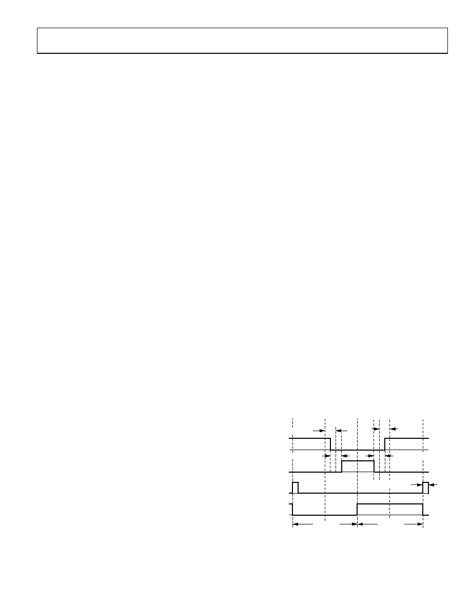
Figure 69 shows a typical pair of PWM outputs (in this case,
0H and 0L) from the timing unit in single update mode. All
illustrated time values indicate the integer value in the
associated register and can be converted to time by simply
multiplying by the fundamental time increment, tCORE. Note
that the switching patterns are perfectly symmetrical about the
midpoint of the switching period in this mode because the same
values of PWMCH0, PWMDAT0, and PWMDAT1 are used to
define the signals in both half cycles of the period.
Figure 69 also demonstrates how the programmed duty cycles
are adjusted to incorporate the desired dead time into the
resulting pair of PWM signals. The dead time is incorporated
by moving the switching instants of both PWM signals (0H and
0L) away from the instant set by the PWMCH0 register.
0
49
55
-02
8
–PWMDAT0 ÷ 2
0H
0L
PWMSYNC
PWMSTA (0)
PWMDAT0
+PWMDAT0 ÷ 2
–PWMDAT0 ÷ 2
00
PWMDAT0
PWMDAT2 + 1
PWMCH0
2 × PWMDAT1
PWMCH0
Figure 69. Typical PWM Outputs of the 3-Phase Timing Unit
(Single Update Mode)
相关PDF资料 |
PDF描述 |
|---|---|
| VI-B2M-IY-F3 | CONVERTER MOD DC/DC 10V 50W |
| MUSB-2A111-024BP | DUST COVER FOR MUSB TYPE A BLACK |
| VI-B2M-IY-F2 | CONVERTER MOD DC/DC 10V 50W |
| AT89C51AC3-S3SUM | IC 8051 MCU 64K FLASH 52-PLCC |
| VI-B2M-IY-F1 | CONVERTER MOD DC/DC 10V 50W |
相关代理商/技术参数 |
参数描述 |
|---|---|
| ADUC7021BCPZ62I | 功能描述:IC MCU FLSH 62K ANLG I/O 40LFCSP RoHS:是 类别:集成电路 (IC) >> 嵌入式 - 微控制器, 系列:MicroConverter® ADuC7xxx 产品培训模块:MCU Product Line Introduction XMEGA Introduction AVR XMEGA USB Connectivity 标准包装:90 系列:AVR® XMEGA 核心处理器:AVR 芯体尺寸:8/16-位 速度:32MHz 连通性:I²C,IrDA,SPI,UART/USART 外围设备:欠压检测/复位,DMA,POR,PWM,WDT 输入/输出数:50 程序存储器容量:192KB(96K x 16) 程序存储器类型:闪存 EEPROM 大小:4K x 8 RAM 容量:16K x 8 电压 - 电源 (Vcc/Vdd):1.6 V ~ 3.6 V 数据转换器:A/D 16x12b; D/A 2x12b 振荡器型:内部 工作温度:-40°C ~ 85°C 封装/外壳:64-TQFP 包装:托盘 配用:ATSTK600-RC14-ND - STK600 SOCKET/ADAPTER 64TQFPATSTK600-TQFP64-ND - STK600 SOCKET/ADAPTER 64-TQFPATAVRONEKIT-ND - KIT AVR/AVR32 DEBUGGER/PROGRMMRATAVRISP2-ND - PROGRAMMER AVR IN SYSTEM |
| ADUC7021BCPZ62I-RL | 功能描述:IC MCU 12BIT 1MSPS I2C 40-LFCSP RoHS:是 类别:集成电路 (IC) >> 嵌入式 - 微控制器, 系列:MicroConverter® ADuC7xxx 标准包装:38 系列:Encore!® XP® 核心处理器:eZ8 芯体尺寸:8-位 速度:5MHz 连通性:IrDA,UART/USART 外围设备:欠压检测/复位,LED,POR,PWM,WDT 输入/输出数:16 程序存储器容量:4KB(4K x 8) 程序存储器类型:闪存 EEPROM 大小:- RAM 容量:1K x 8 电压 - 电源 (Vcc/Vdd):2.7 V ~ 3.6 V 数据转换器:- 振荡器型:内部 工作温度:-40°C ~ 105°C 封装/外壳:20-SOIC(0.295",7.50mm 宽) 包装:管件 其它名称:269-4116Z8F0413SH005EG-ND |
| ADUC7021BCPZ62IRL7 | 制造商:Analog Devices 功能描述:MCU 16-bit/32-bit ADuC7xxx ARM7TDMI RISC 62KB Flash 3.3V 40-Pin LFCSP EP T/R |
| ADUC7021BCPZ62-RL | 功能描述:IC MCU 12BIT 1MSPS UART 40-LFCSP RoHS:是 类别:集成电路 (IC) >> 嵌入式 - 微控制器, 系列:MicroConverter® ADuC7xxx 标准包装:38 系列:Encore!® XP® 核心处理器:eZ8 芯体尺寸:8-位 速度:5MHz 连通性:IrDA,UART/USART 外围设备:欠压检测/复位,LED,POR,PWM,WDT 输入/输出数:16 程序存储器容量:4KB(4K x 8) 程序存储器类型:闪存 EEPROM 大小:- RAM 容量:1K x 8 电压 - 电源 (Vcc/Vdd):2.7 V ~ 3.6 V 数据转换器:- 振荡器型:内部 工作温度:-40°C ~ 105°C 封装/外壳:20-SOIC(0.295",7.50mm 宽) 包装:管件 其它名称:269-4116Z8F0413SH005EG-ND |
| ADUC7021BCPZ62-RL7 | 功能描述:IC MCU 12BIT 1MSPS UART 40-LFCSP RoHS:是 类别:集成电路 (IC) >> 嵌入式 - 微控制器, 系列:MicroConverter® ADuC7xxx 标准包装:38 系列:Encore!® XP® 核心处理器:eZ8 芯体尺寸:8-位 速度:5MHz 连通性:IrDA,UART/USART 外围设备:欠压检测/复位,LED,POR,PWM,WDT 输入/输出数:16 程序存储器容量:4KB(4K x 8) 程序存储器类型:闪存 EEPROM 大小:- RAM 容量:1K x 8 电压 - 电源 (Vcc/Vdd):2.7 V ~ 3.6 V 数据转换器:- 振荡器型:内部 工作温度:-40°C ~ 105°C 封装/外壳:20-SOIC(0.295",7.50mm 宽) 包装:管件 其它名称:269-4116Z8F0413SH005EG-ND |
发布紧急采购,3分钟左右您将得到回复。