- 您现在的位置:买卖IC网 > PDF目录12027 > ADUC7021BCPZ62 (Analog Devices Inc)IC MCU FLSH 62K ANLG I/O 40LFCSP PDF资料下载
参数资料
| 型号: | ADUC7021BCPZ62 |
| 厂商: | Analog Devices Inc |
| 文件页数: | 92/104页 |
| 文件大小: | 0K |
| 描述: | IC MCU FLSH 62K ANLG I/O 40LFCSP |
| 产品培训模块: | ARM7 Applications & Tools Process Control |
| 标准包装: | 1 |
| 系列: | MicroConverter® ADuC7xxx |
| 核心处理器: | ARM7 |
| 芯体尺寸: | 16/32-位 |
| 速度: | 44MHz |
| 连通性: | EBI/EMI,I²C,SPI,UART/USART |
| 外围设备: | PLA,PWM,PSM,温度传感器,WDT |
| 输入/输出数: | 13 |
| 程序存储器容量: | 64KB(32K x 16) |
| 程序存储器类型: | 闪存 |
| RAM 容量: | 2K x 32 |
| 电压 - 电源 (Vcc/Vdd): | 2.7 V ~ 3.6 V |
| 数据转换器: | A/D 8x12b,D/A 2x12b |
| 振荡器型: | 内部 |
| 工作温度: | -40°C ~ 125°C |
| 封装/外壳: | 40-VFQFN 裸露焊盘,CSP |
| 包装: | 托盘 |
第1页第2页第3页第4页第5页第6页第7页第8页第9页第10页第11页第12页第13页第14页第15页第16页第17页第18页第19页第20页第21页第22页第23页第24页第25页第26页第27页第28页第29页第30页第31页第32页第33页第34页第35页第36页第37页第38页第39页第40页第41页第42页第43页第44页第45页第46页第47页第48页第49页第50页第51页第52页第53页第54页第55页第56页第57页第58页第59页第60页第61页第62页第63页第64页第65页第66页第67页第68页第69页第70页第71页第72页第73页第74页第75页第76页第77页第78页第79页第80页第81页第82页第83页第84页第85页第86页第87页第88页第89页第90页第91页当前第92页第93页第94页第95页第96页第97页第98页第99页第100页第101页第102页第103页第104页
ADuC7019/20/21/22/24/25/26/27/28/29
Data Sheet
Rev. F | Page 88 of 104
Table 186. T2CON MMR Bit Descriptions
Bit
Value
Description
31:11
Reserved.
10:9
Clock source.
00
External crystal.
01
External crystal.
10
Internal oscillator.
11
Core clock (41 MHz/2CD).
8
Count up. Set by user for Timer2 to count up.
Cleared by user for Timer2 to count down by
default.
7
Timer2 enable bit. Set by user to enable Timer2.
Cleared by user to disable Timer2 by default.
6
Timer2 mode. Set by user to operate in
periodic mode. Cleared by user to operate in
free-running mode. Default mode.
5:4
Format.
00
Binary.
01
Reserved.
10
Hr: min: sec: Hundredths (23 hours to 0 hour).
11
Hr: min: sec: Hundredths (255 hours to 0 hour).
3:0
Prescale.
0000
Source Clock/1 by default.
0100
Source Clock/16.
1000
Source Clock/256 expected for Format 2 and
Format 3.
1111
Source Clock/32,768.
Table 187. T2CLRI Register
Name
Address
Default Value
Access
T2CLRI
0xFFFF034C
0xFF
W
T2CLRI is an 8-bit register. Writing any value to this register
clears the Timer2 interrupt.
Timer3 (Watchdog Timer)
Timer3 has two modes of operation: normal mode and
watchdog mode. The watchdog timer is used to recover from
an illegal software state. Once enabled, it requires periodic
servicing to prevent it from forcing a processor reset.
Normal Mode
Timer3 in normal mode is identical to Timer0, except for the
clock source and the count-up functionality. The clock source
is 32 kHz from the PLL and can be scaled by a factor of 1, 16,
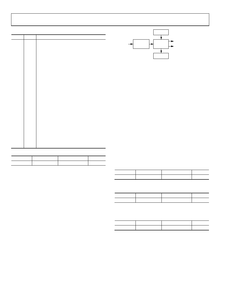
or 256 (see Figure 80).
04955-
037
32.768kHz
PRESCALER
/1, 16 OR 256
16-BIT
UP/DOWN
COUNTER
16-BIT
LOAD
TIMER3
VALUE
WATCHDOG
RESET
TIMER3 IRQ
Figure 80. Timer3 Block Diagram
Watchdog Mode
Watchdog mode is entered by setting Bit 5 in the T3CON MMR.
Timer3 decreases from the value present in the T3LD register to 0.
T3LD is used as the timeout. The maximum timeout can be
512 sec, using the prescaler/256, and full scale in T3LD. Timer3
is clocked by the internal 32 kHz crystal when operating in
watchdog mode. Note that to enter watchdog mode success-
fully, Bit 5 in the T3CON MMR must be set after writing to the
T3LD MMR.
If the timer reaches 0, a reset or an interrupt occurs, depending
on Bit 1 in the T3CON register. To avoid reset or interrupt, any
value must be written to T3CLRI before the expiration period.
This reloads the counter with T3LD and begins a new timeout
period.
When watchdog mode is entered, T3LD and T3CON are write-
protected. These two registers cannot be modified until a reset
clears the watchdog enable bit, which causes Timer3 to exit
watchdog mode.
The Timer3 interface consists of four MMRs: T3LD, T3VAL,
T3CON, and T3CLRI.
Table 188. T3LD Register
Name
Address
Default Value
Access
T3LD
0xFFFF0360
0x0000
R/W
T3LD is a 16-bit register load register.
Table 189. T3VAL Register
Name
Address
Default Value
Access
T3VAL
0xFFFF0364
0xFFFF
R
T3VAL is a 16-bit read-only register that represents the current
state of the counter.
Table 190. T3CON Register
Name
Address
Default Value
Access
T3CON
0xFFFF0368
0x0000
R/W
T3CON is the configuration MMR described in Table 191.
相关PDF资料 |
PDF描述 |
|---|---|
| VI-B2M-IY-F3 | CONVERTER MOD DC/DC 10V 50W |
| MUSB-2A111-024BP | DUST COVER FOR MUSB TYPE A BLACK |
| VI-B2M-IY-F2 | CONVERTER MOD DC/DC 10V 50W |
| AT89C51AC3-S3SUM | IC 8051 MCU 64K FLASH 52-PLCC |
| VI-B2M-IY-F1 | CONVERTER MOD DC/DC 10V 50W |
相关代理商/技术参数 |
参数描述 |
|---|---|
| ADUC7021BCPZ62I | 功能描述:IC MCU FLSH 62K ANLG I/O 40LFCSP RoHS:是 类别:集成电路 (IC) >> 嵌入式 - 微控制器, 系列:MicroConverter® ADuC7xxx 产品培训模块:MCU Product Line Introduction XMEGA Introduction AVR XMEGA USB Connectivity 标准包装:90 系列:AVR® XMEGA 核心处理器:AVR 芯体尺寸:8/16-位 速度:32MHz 连通性:I²C,IrDA,SPI,UART/USART 外围设备:欠压检测/复位,DMA,POR,PWM,WDT 输入/输出数:50 程序存储器容量:192KB(96K x 16) 程序存储器类型:闪存 EEPROM 大小:4K x 8 RAM 容量:16K x 8 电压 - 电源 (Vcc/Vdd):1.6 V ~ 3.6 V 数据转换器:A/D 16x12b; D/A 2x12b 振荡器型:内部 工作温度:-40°C ~ 85°C 封装/外壳:64-TQFP 包装:托盘 配用:ATSTK600-RC14-ND - STK600 SOCKET/ADAPTER 64TQFPATSTK600-TQFP64-ND - STK600 SOCKET/ADAPTER 64-TQFPATAVRONEKIT-ND - KIT AVR/AVR32 DEBUGGER/PROGRMMRATAVRISP2-ND - PROGRAMMER AVR IN SYSTEM |
| ADUC7021BCPZ62I-RL | 功能描述:IC MCU 12BIT 1MSPS I2C 40-LFCSP RoHS:是 类别:集成电路 (IC) >> 嵌入式 - 微控制器, 系列:MicroConverter® ADuC7xxx 标准包装:38 系列:Encore!® XP® 核心处理器:eZ8 芯体尺寸:8-位 速度:5MHz 连通性:IrDA,UART/USART 外围设备:欠压检测/复位,LED,POR,PWM,WDT 输入/输出数:16 程序存储器容量:4KB(4K x 8) 程序存储器类型:闪存 EEPROM 大小:- RAM 容量:1K x 8 电压 - 电源 (Vcc/Vdd):2.7 V ~ 3.6 V 数据转换器:- 振荡器型:内部 工作温度:-40°C ~ 105°C 封装/外壳:20-SOIC(0.295",7.50mm 宽) 包装:管件 其它名称:269-4116Z8F0413SH005EG-ND |
| ADUC7021BCPZ62IRL7 | 制造商:Analog Devices 功能描述:MCU 16-bit/32-bit ADuC7xxx ARM7TDMI RISC 62KB Flash 3.3V 40-Pin LFCSP EP T/R |
| ADUC7021BCPZ62-RL | 功能描述:IC MCU 12BIT 1MSPS UART 40-LFCSP RoHS:是 类别:集成电路 (IC) >> 嵌入式 - 微控制器, 系列:MicroConverter® ADuC7xxx 标准包装:38 系列:Encore!® XP® 核心处理器:eZ8 芯体尺寸:8-位 速度:5MHz 连通性:IrDA,UART/USART 外围设备:欠压检测/复位,LED,POR,PWM,WDT 输入/输出数:16 程序存储器容量:4KB(4K x 8) 程序存储器类型:闪存 EEPROM 大小:- RAM 容量:1K x 8 电压 - 电源 (Vcc/Vdd):2.7 V ~ 3.6 V 数据转换器:- 振荡器型:内部 工作温度:-40°C ~ 105°C 封装/外壳:20-SOIC(0.295",7.50mm 宽) 包装:管件 其它名称:269-4116Z8F0413SH005EG-ND |
| ADUC7021BCPZ62-RL7 | 功能描述:IC MCU 12BIT 1MSPS UART 40-LFCSP RoHS:是 类别:集成电路 (IC) >> 嵌入式 - 微控制器, 系列:MicroConverter® ADuC7xxx 标准包装:38 系列:Encore!® XP® 核心处理器:eZ8 芯体尺寸:8-位 速度:5MHz 连通性:IrDA,UART/USART 外围设备:欠压检测/复位,LED,POR,PWM,WDT 输入/输出数:16 程序存储器容量:4KB(4K x 8) 程序存储器类型:闪存 EEPROM 大小:- RAM 容量:1K x 8 电压 - 电源 (Vcc/Vdd):2.7 V ~ 3.6 V 数据转换器:- 振荡器型:内部 工作温度:-40°C ~ 105°C 封装/外壳:20-SOIC(0.295",7.50mm 宽) 包装:管件 其它名称:269-4116Z8F0413SH005EG-ND |
发布紧急采购,3分钟左右您将得到回复。