- 您现在的位置:买卖IC网 > PDF目录12027 > ADUC7021BCPZ62 (Analog Devices Inc)IC MCU FLSH 62K ANLG I/O 40LFCSP PDF资料下载
参数资料
| 型号: | ADUC7021BCPZ62 |
| 厂商: | Analog Devices Inc |
| 文件页数: | 59/104页 |
| 文件大小: | 0K |
| 描述: | IC MCU FLSH 62K ANLG I/O 40LFCSP |
| 产品培训模块: | ARM7 Applications & Tools Process Control |
| 标准包装: | 1 |
| 系列: | MicroConverter® ADuC7xxx |
| 核心处理器: | ARM7 |
| 芯体尺寸: | 16/32-位 |
| 速度: | 44MHz |
| 连通性: | EBI/EMI,I²C,SPI,UART/USART |
| 外围设备: | PLA,PWM,PSM,温度传感器,WDT |
| 输入/输出数: | 13 |
| 程序存储器容量: | 64KB(32K x 16) |
| 程序存储器类型: | 闪存 |
| RAM 容量: | 2K x 32 |
| 电压 - 电源 (Vcc/Vdd): | 2.7 V ~ 3.6 V |
| 数据转换器: | A/D 8x12b,D/A 2x12b |
| 振荡器型: | 内部 |
| 工作温度: | -40°C ~ 125°C |
| 封装/外壳: | 40-VFQFN 裸露焊盘,CSP |
| 包装: | 托盘 |
第1页第2页第3页第4页第5页第6页第7页第8页第9页第10页第11页第12页第13页第14页第15页第16页第17页第18页第19页第20页第21页第22页第23页第24页第25页第26页第27页第28页第29页第30页第31页第32页第33页第34页第35页第36页第37页第38页第39页第40页第41页第42页第43页第44页第45页第46页第47页第48页第49页第50页第51页第52页第53页第54页第55页第56页第57页第58页当前第59页第60页第61页第62页第63页第64页第65页第66页第67页第68页第69页第70页第71页第72页第73页第74页第75页第76页第77页第78页第79页第80页第81页第82页第83页第84页第85页第86页第87页第88页第89页第90页第91页第92页第93页第94页第95页第96页第97页第98页第99页第100页第101页第102页第103页第104页
ADuC7019/20/21/22/24/25/26/27/28/29
Data Sheet
Rev. F | Page 58 of 104
Input offset voltage (VOS) is the difference between the center of
the hysteresis range and the ground level. This can either be
positive or negative. The hysteresis voltage (VH) is one-half the
width of the hysteresis range.
Comparator Interface
The comparator interface consists of a 16-bit MMR, CMPCON,
which is described in Table 56.
Table 55. CMPCON Register
Name
Address
Default Value
Access
CMPCON
0xFFFF0444
0x0000
R/W
Table 56. CMPCON MMR Bit Descriptions
Bit
Name
Value
Description
15:11
Reserved.
10
CMPEN
Comparator enable bit. Set by user
to enable the comparator. Cleared
by user to disable the comparator.
9:8
CMPIN
Comparator negative input
select bits.
00
AVDD/2.
01
ADC3 input.
10
DAC0 output.
11
Reserved.
7:6
CMPOC
Comparator output configuration
bits.
00
Reserved.
01
Reserved.
10
Output on CMPOUT.
11
IRQ.
5
CMPOL
Comparator output logic state bit.
When low, the comparator output
is high if the positive input (CMP0)
is above the negative input (CMP1).
When high, the comparator output
is high if the positive input is below
the negative input.
4:3
CMPRES
Response time.
00
5 s response time is typical for
large signals (2.5 V differential).
17 s response time is typical for
small signals (0.65 mV differential).
11
3 s typical.
01/10
Reserved.
2
CMPHYST
Comparator hysteresis bit. Set by
user to have a hysteresis of about
7.5 mV. Cleared by user to have no
hysteresis.
1
CMPORI
Comparator output rising edge
interrupt. Set automatically when a
rising edge occurs on the moni-
tored voltage (CMP0). Cleared by
user by writing a 1 to this bit.
0
CMPOFI
Comparator output falling edge
interrupt. Set automatically when a
falling edge occurs on the monitored
voltage (CMP0). Cleared by user.
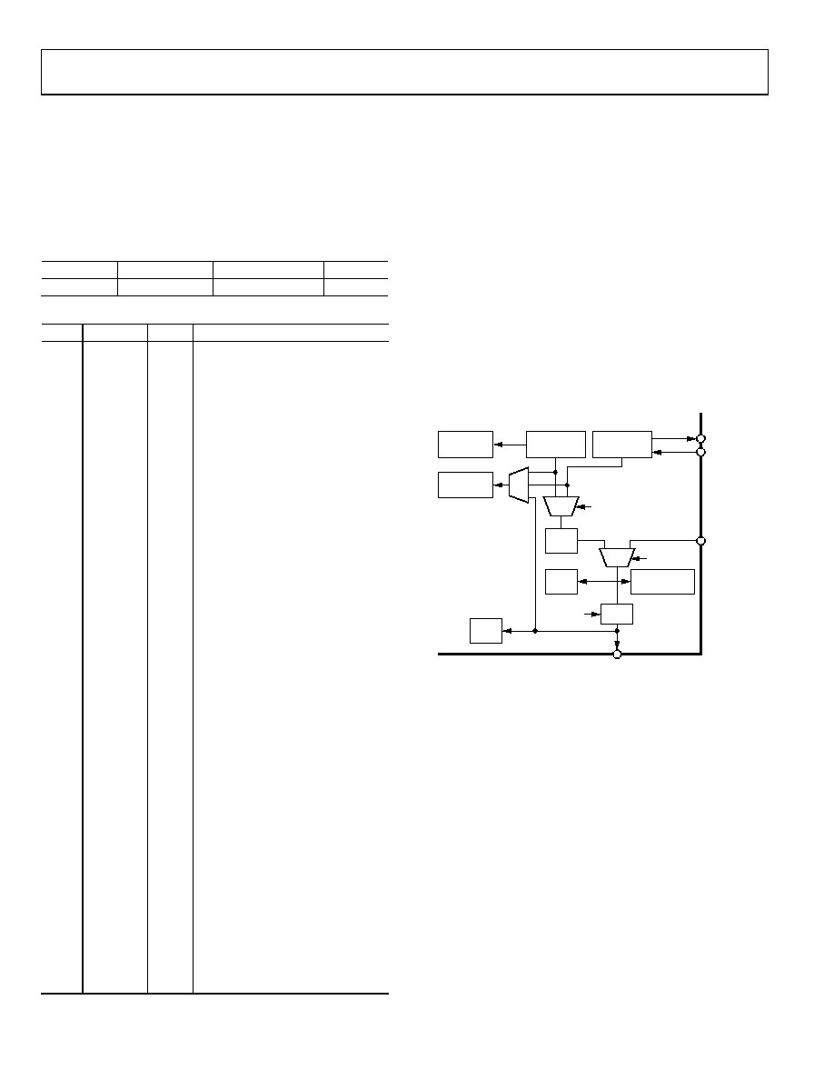
OSCILLATOR AND PLL—POWER CONTROL
Clocking System
Each ADuC7019/20/21/22/24/25/26/27/28/29 integrates a
32.768 kHz ±3% oscillator, a clock divider, and a PLL. The PLL
locks onto a multiple (1275) of the internal oscillator or an external
32.768 kHz crystal to provide a stable 41.78 MHz clock (UCLK) for
the system. To allow power saving, the core can operate at this
frequency, or at binary submultiples of it. The actual core oper-
ating frequency, UCLK/2CD, is refered to as HCLK. The default
core clock is the PLL clock divided by 8 (CD = 3) or 5.22 MHz.
The core clock frequency can also come from an external clock
on the ECLK pin as described in Figure 67. The core clock can
be outputted on ECLK when using an internal oscillator or
external crystal.
Note that when the ECLK pin is used to output the core clock,
the output signal is not buffered and is not suitable for use as a
clock source to an external device without an external buffer.
04955-
026
*32.768kHz ±3%
AT POWER-UP
41.78MHz
OCLK
32.768kHz
WATCHDOG
TIMER
INT. 32kHz*
OSCILLATOR
CRYSTAL
OSCILLATOR
WAKE-UP
TIMER
MDCLK
HCLK
PLL
CORE
I2C
UCLK
ANALOG
PERIPHERALS
/2CD
CD
XCLKO
XCLKI
P0.7/XCLK
P0.7/ECLK
Figure 67. Clocking System
The selection of the clock source is in the PLLCON register. By
default, the part uses the internal oscillator feeding the PLL.
External Crystal Selection
To switch to an external crystal, the user must do the following:
1. Enable the Timer2 interrupt and configure it for a timeout
period of >120 s.
2. Follow the write sequence to the PLLCON register, setting
the MDCLK bits to 01 and clearing the OSEL bit.
3. Force the part into NAP mode by following the correct
write sequence to the POWCON register.
When the part is interrupted from NAP mode by the
Timer2 interrupt source, the clock source has switched to
the external clock.
相关PDF资料 |
PDF描述 |
|---|---|
| VI-B2M-IY-F3 | CONVERTER MOD DC/DC 10V 50W |
| MUSB-2A111-024BP | DUST COVER FOR MUSB TYPE A BLACK |
| VI-B2M-IY-F2 | CONVERTER MOD DC/DC 10V 50W |
| AT89C51AC3-S3SUM | IC 8051 MCU 64K FLASH 52-PLCC |
| VI-B2M-IY-F1 | CONVERTER MOD DC/DC 10V 50W |
相关代理商/技术参数 |
参数描述 |
|---|---|
| ADUC7021BCPZ62I | 功能描述:IC MCU FLSH 62K ANLG I/O 40LFCSP RoHS:是 类别:集成电路 (IC) >> 嵌入式 - 微控制器, 系列:MicroConverter® ADuC7xxx 产品培训模块:MCU Product Line Introduction XMEGA Introduction AVR XMEGA USB Connectivity 标准包装:90 系列:AVR® XMEGA 核心处理器:AVR 芯体尺寸:8/16-位 速度:32MHz 连通性:I²C,IrDA,SPI,UART/USART 外围设备:欠压检测/复位,DMA,POR,PWM,WDT 输入/输出数:50 程序存储器容量:192KB(96K x 16) 程序存储器类型:闪存 EEPROM 大小:4K x 8 RAM 容量:16K x 8 电压 - 电源 (Vcc/Vdd):1.6 V ~ 3.6 V 数据转换器:A/D 16x12b; D/A 2x12b 振荡器型:内部 工作温度:-40°C ~ 85°C 封装/外壳:64-TQFP 包装:托盘 配用:ATSTK600-RC14-ND - STK600 SOCKET/ADAPTER 64TQFPATSTK600-TQFP64-ND - STK600 SOCKET/ADAPTER 64-TQFPATAVRONEKIT-ND - KIT AVR/AVR32 DEBUGGER/PROGRMMRATAVRISP2-ND - PROGRAMMER AVR IN SYSTEM |
| ADUC7021BCPZ62I-RL | 功能描述:IC MCU 12BIT 1MSPS I2C 40-LFCSP RoHS:是 类别:集成电路 (IC) >> 嵌入式 - 微控制器, 系列:MicroConverter® ADuC7xxx 标准包装:38 系列:Encore!® XP® 核心处理器:eZ8 芯体尺寸:8-位 速度:5MHz 连通性:IrDA,UART/USART 外围设备:欠压检测/复位,LED,POR,PWM,WDT 输入/输出数:16 程序存储器容量:4KB(4K x 8) 程序存储器类型:闪存 EEPROM 大小:- RAM 容量:1K x 8 电压 - 电源 (Vcc/Vdd):2.7 V ~ 3.6 V 数据转换器:- 振荡器型:内部 工作温度:-40°C ~ 105°C 封装/外壳:20-SOIC(0.295",7.50mm 宽) 包装:管件 其它名称:269-4116Z8F0413SH005EG-ND |
| ADUC7021BCPZ62IRL7 | 制造商:Analog Devices 功能描述:MCU 16-bit/32-bit ADuC7xxx ARM7TDMI RISC 62KB Flash 3.3V 40-Pin LFCSP EP T/R |
| ADUC7021BCPZ62-RL | 功能描述:IC MCU 12BIT 1MSPS UART 40-LFCSP RoHS:是 类别:集成电路 (IC) >> 嵌入式 - 微控制器, 系列:MicroConverter® ADuC7xxx 标准包装:38 系列:Encore!® XP® 核心处理器:eZ8 芯体尺寸:8-位 速度:5MHz 连通性:IrDA,UART/USART 外围设备:欠压检测/复位,LED,POR,PWM,WDT 输入/输出数:16 程序存储器容量:4KB(4K x 8) 程序存储器类型:闪存 EEPROM 大小:- RAM 容量:1K x 8 电压 - 电源 (Vcc/Vdd):2.7 V ~ 3.6 V 数据转换器:- 振荡器型:内部 工作温度:-40°C ~ 105°C 封装/外壳:20-SOIC(0.295",7.50mm 宽) 包装:管件 其它名称:269-4116Z8F0413SH005EG-ND |
| ADUC7021BCPZ62-RL7 | 功能描述:IC MCU 12BIT 1MSPS UART 40-LFCSP RoHS:是 类别:集成电路 (IC) >> 嵌入式 - 微控制器, 系列:MicroConverter® ADuC7xxx 标准包装:38 系列:Encore!® XP® 核心处理器:eZ8 芯体尺寸:8-位 速度:5MHz 连通性:IrDA,UART/USART 外围设备:欠压检测/复位,LED,POR,PWM,WDT 输入/输出数:16 程序存储器容量:4KB(4K x 8) 程序存储器类型:闪存 EEPROM 大小:- RAM 容量:1K x 8 电压 - 电源 (Vcc/Vdd):2.7 V ~ 3.6 V 数据转换器:- 振荡器型:内部 工作温度:-40°C ~ 105°C 封装/外壳:20-SOIC(0.295",7.50mm 宽) 包装:管件 其它名称:269-4116Z8F0413SH005EG-ND |
发布紧急采购,3分钟左右您将得到回复。