- 您现在的位置:买卖IC网 > PDF目录12027 > ADUC7021BCPZ62 (Analog Devices Inc)IC MCU FLSH 62K ANLG I/O 40LFCSP PDF资料下载
参数资料
| 型号: | ADUC7021BCPZ62 |
| 厂商: | Analog Devices Inc |
| 文件页数: | 79/104页 |
| 文件大小: | 0K |
| 描述: | IC MCU FLSH 62K ANLG I/O 40LFCSP |
| 产品培训模块: | ARM7 Applications & Tools Process Control |
| 标准包装: | 1 |
| 系列: | MicroConverter® ADuC7xxx |
| 核心处理器: | ARM7 |
| 芯体尺寸: | 16/32-位 |
| 速度: | 44MHz |
| 连通性: | EBI/EMI,I²C,SPI,UART/USART |
| 外围设备: | PLA,PWM,PSM,温度传感器,WDT |
| 输入/输出数: | 13 |
| 程序存储器容量: | 64KB(32K x 16) |
| 程序存储器类型: | 闪存 |
| RAM 容量: | 2K x 32 |
| 电压 - 电源 (Vcc/Vdd): | 2.7 V ~ 3.6 V |
| 数据转换器: | A/D 8x12b,D/A 2x12b |
| 振荡器型: | 内部 |
| 工作温度: | -40°C ~ 125°C |
| 封装/外壳: | 40-VFQFN 裸露焊盘,CSP |
| 包装: | 托盘 |
第1页第2页第3页第4页第5页第6页第7页第8页第9页第10页第11页第12页第13页第14页第15页第16页第17页第18页第19页第20页第21页第22页第23页第24页第25页第26页第27页第28页第29页第30页第31页第32页第33页第34页第35页第36页第37页第38页第39页第40页第41页第42页第43页第44页第45页第46页第47页第48页第49页第50页第51页第52页第53页第54页第55页第56页第57页第58页第59页第60页第61页第62页第63页第64页第65页第66页第67页第68页第69页第70页第71页第72页第73页第74页第75页第76页第77页第78页当前第79页第80页第81页第82页第83页第84页第85页第86页第87页第88页第89页第90页第91页第92页第93页第94页第95页第96页第97页第98页第99页第100页第101页第102页第103页第104页
ADuC7019/20/21/22/24/25/26/27/28/29
Data Sheet
Rev. F | Page 76 of 104
I2C-COMPATIBLE INTERFACES
The ADuC7019/20/21/22/24/25/26/27/28/29 support two licensed
I2C interfaces. The I2C interfaces are both implemented as a hard-
ware master and a full slave interface. Because the two I2C inter-
faces are identical, this data sheet describes only I2C0 in detail.
Note that the two masters and one of the slaves have individual
interrupts (see the Interrupt System section).
Note that when configured as an I2C master device, the
ADuC7019/20/21/22/24/25/26/27/28/29 cannot generate a
repeated start condition.
The two GPIO pins used for data transfer, SDAx and SCLx, are
configured in a wired-AND format that allows arbitration in a
multimaster system. These pins require external pull-up resistors.
Typical pull-up values are 10 k.
The I2C bus peripheral address in the I2C bus system is pro-
grammed by the user. This ID can be modified any time a
transfer is not in progress. The user can configure the interface
to respond to four slave addresses.
The transfer sequence of an I2C system consists of a master
device initiating a transfer by generating a start condition while
the bus is idle. The master transmits the slave device address
and the direction of the data transfer during the initial address
transfer. If the master does not lose arbitration and the slave
acknowledges, the data transfer is initiated. This continues until
the master issues a stop condition and the bus becomes idle.
The I2C peripheral can be configured only as a master or slave
at any given time. The same I2C channel cannot simultaneously
support master and slave modes.
Serial Clock Generation
The I2C master in the system generates the serial clock for a
transfer. The master channel can be configured to operate in
fast mode (400 kHz) or standard mode (100 kHz).
The bit rate is defined in the I2C0DIV MMR as follows:
)
(2
)
2
(
DIVL
DIVH
+
=
UCLK
CLOCK
SERIAL
f
where:
fUCLK = clock before the clock divider.
DIVH = the high period of the clock.
DIVL = the low period of the clock.
Thus, for 100 kHz operation,
DIVH = DIVL = 0xCF
and for 400 kHz,
DIVH = 0x28, DIVL = 0x3C
The I2CxDIV registers correspond to DIVH:DIVL.
Slave Addresses
The registers I2C0ID0, I2C0ID1, I2C0ID2, and I2C0ID3 contain
the device IDs. The device compares the four I2C0IDx registers
to the address byte. To be correctly addressed, the seven MSBs of
either ID register must be identical to that of the seven MSBs of
the first received address byte. The LSB of the ID registers (the
transfer direction bit) is ignored in the process of address
recognition.
I2C Registers
The I2C peripheral interface consists of 18 MMRs, which are
discussed in this section.
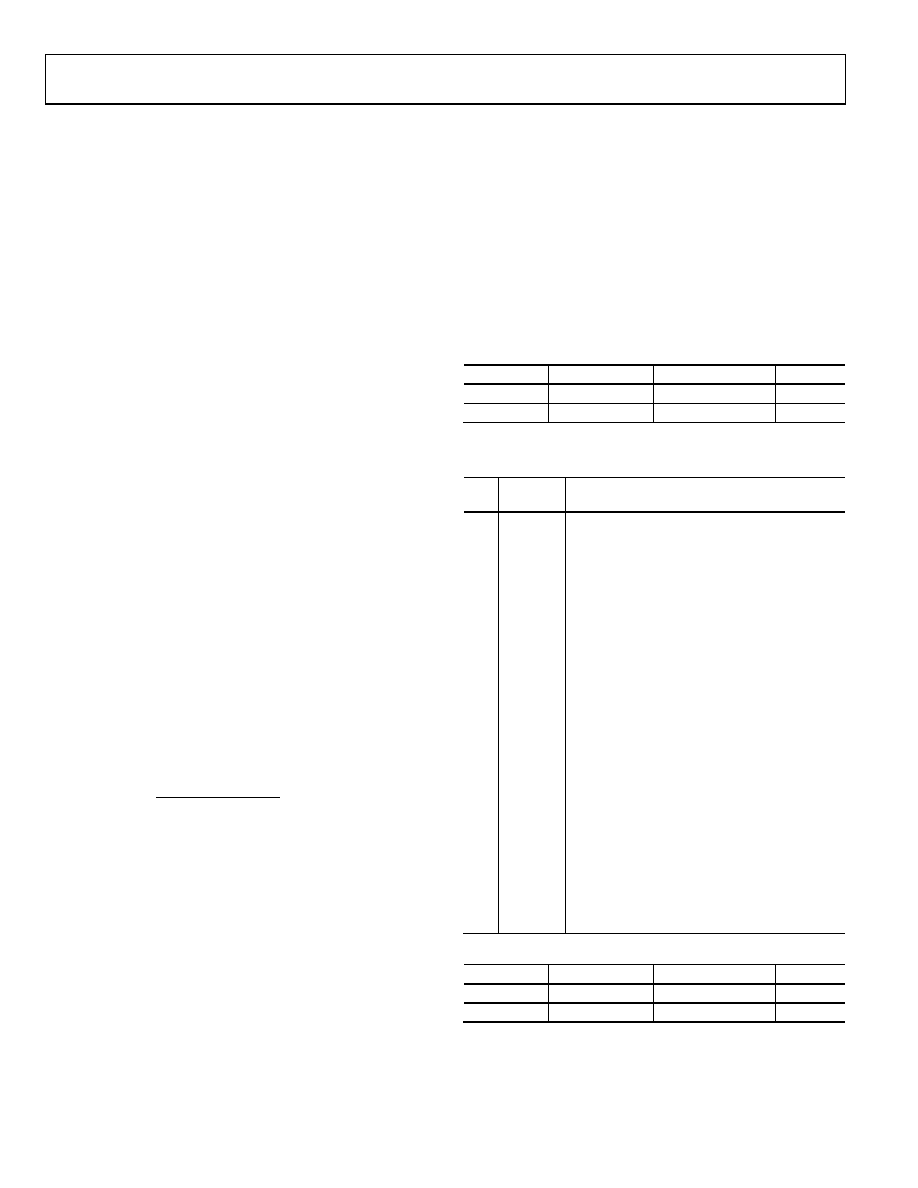
Table 126. I2CxMSTA Registers
Name
Address
Default Value
Access
I2C0MSTA
0xFFFF0800
0x00
R/W
I2C1MSTA
0xFFFF0900
0x00
R/W
I2CxMSTA are status registers for the master channel.
Table 127. I2C0MSTA MMR Bit Descriptions
Bit
Access
Type
Description
7
R/W
Master transmit FIFO flush. Set by user to flush
the master Tx FIFO. Cleared automatically after
the master Tx FIFO is flushed. This bit also
flushes the slave receive FIFO.
6
R
Master busy. Set automatically if the master is
busy. Cleared automatically.
5
R
Arbitration loss. Set in multimaster mode if
another master has the bus. Cleared when the
bus becomes available.
4
R
No ACK. Set automatically if there is no
acknowledge of the address by the slave
device. Cleared automatically by reading the
I2C0MSTA register.
3
R
Master receive IRQ. Set after receiving data.
Cleared automatically by reading the I2C0MRX
register.
2
R
Master transmit IRQ. Set at the end of a
transmission. Cleared automatically by writing
to the I2C0MTX register.
1
R
Master transmit FIFO underflow. Set
automatically if the master transmit FIFO is
underflowing. Cleared automatically by
writing to the I2C0MTX register.
0
R
Master TX FIFO not full. Set automatically if the
slave transmit FIFO is not full. Cleared automati-
cally by writing twice to the I2C0STX register.
Table 128. I2CxSSTA Registers
Name
Address
Default Value
Access
I2C0SSTA
0xFFFF0804
0x01
R
I2C1SSTA
0xFFFF0904
0x01
R
I2CxSSTA are status registers for the slave channel.
相关PDF资料 |
PDF描述 |
|---|---|
| VI-B2M-IY-F3 | CONVERTER MOD DC/DC 10V 50W |
| MUSB-2A111-024BP | DUST COVER FOR MUSB TYPE A BLACK |
| VI-B2M-IY-F2 | CONVERTER MOD DC/DC 10V 50W |
| AT89C51AC3-S3SUM | IC 8051 MCU 64K FLASH 52-PLCC |
| VI-B2M-IY-F1 | CONVERTER MOD DC/DC 10V 50W |
相关代理商/技术参数 |
参数描述 |
|---|---|
| ADUC7021BCPZ62I | 功能描述:IC MCU FLSH 62K ANLG I/O 40LFCSP RoHS:是 类别:集成电路 (IC) >> 嵌入式 - 微控制器, 系列:MicroConverter® ADuC7xxx 产品培训模块:MCU Product Line Introduction XMEGA Introduction AVR XMEGA USB Connectivity 标准包装:90 系列:AVR® XMEGA 核心处理器:AVR 芯体尺寸:8/16-位 速度:32MHz 连通性:I²C,IrDA,SPI,UART/USART 外围设备:欠压检测/复位,DMA,POR,PWM,WDT 输入/输出数:50 程序存储器容量:192KB(96K x 16) 程序存储器类型:闪存 EEPROM 大小:4K x 8 RAM 容量:16K x 8 电压 - 电源 (Vcc/Vdd):1.6 V ~ 3.6 V 数据转换器:A/D 16x12b; D/A 2x12b 振荡器型:内部 工作温度:-40°C ~ 85°C 封装/外壳:64-TQFP 包装:托盘 配用:ATSTK600-RC14-ND - STK600 SOCKET/ADAPTER 64TQFPATSTK600-TQFP64-ND - STK600 SOCKET/ADAPTER 64-TQFPATAVRONEKIT-ND - KIT AVR/AVR32 DEBUGGER/PROGRMMRATAVRISP2-ND - PROGRAMMER AVR IN SYSTEM |
| ADUC7021BCPZ62I-RL | 功能描述:IC MCU 12BIT 1MSPS I2C 40-LFCSP RoHS:是 类别:集成电路 (IC) >> 嵌入式 - 微控制器, 系列:MicroConverter® ADuC7xxx 标准包装:38 系列:Encore!® XP® 核心处理器:eZ8 芯体尺寸:8-位 速度:5MHz 连通性:IrDA,UART/USART 外围设备:欠压检测/复位,LED,POR,PWM,WDT 输入/输出数:16 程序存储器容量:4KB(4K x 8) 程序存储器类型:闪存 EEPROM 大小:- RAM 容量:1K x 8 电压 - 电源 (Vcc/Vdd):2.7 V ~ 3.6 V 数据转换器:- 振荡器型:内部 工作温度:-40°C ~ 105°C 封装/外壳:20-SOIC(0.295",7.50mm 宽) 包装:管件 其它名称:269-4116Z8F0413SH005EG-ND |
| ADUC7021BCPZ62IRL7 | 制造商:Analog Devices 功能描述:MCU 16-bit/32-bit ADuC7xxx ARM7TDMI RISC 62KB Flash 3.3V 40-Pin LFCSP EP T/R |
| ADUC7021BCPZ62-RL | 功能描述:IC MCU 12BIT 1MSPS UART 40-LFCSP RoHS:是 类别:集成电路 (IC) >> 嵌入式 - 微控制器, 系列:MicroConverter® ADuC7xxx 标准包装:38 系列:Encore!® XP® 核心处理器:eZ8 芯体尺寸:8-位 速度:5MHz 连通性:IrDA,UART/USART 外围设备:欠压检测/复位,LED,POR,PWM,WDT 输入/输出数:16 程序存储器容量:4KB(4K x 8) 程序存储器类型:闪存 EEPROM 大小:- RAM 容量:1K x 8 电压 - 电源 (Vcc/Vdd):2.7 V ~ 3.6 V 数据转换器:- 振荡器型:内部 工作温度:-40°C ~ 105°C 封装/外壳:20-SOIC(0.295",7.50mm 宽) 包装:管件 其它名称:269-4116Z8F0413SH005EG-ND |
| ADUC7021BCPZ62-RL7 | 功能描述:IC MCU 12BIT 1MSPS UART 40-LFCSP RoHS:是 类别:集成电路 (IC) >> 嵌入式 - 微控制器, 系列:MicroConverter® ADuC7xxx 标准包装:38 系列:Encore!® XP® 核心处理器:eZ8 芯体尺寸:8-位 速度:5MHz 连通性:IrDA,UART/USART 外围设备:欠压检测/复位,LED,POR,PWM,WDT 输入/输出数:16 程序存储器容量:4KB(4K x 8) 程序存储器类型:闪存 EEPROM 大小:- RAM 容量:1K x 8 电压 - 电源 (Vcc/Vdd):2.7 V ~ 3.6 V 数据转换器:- 振荡器型:内部 工作温度:-40°C ~ 105°C 封装/外壳:20-SOIC(0.295",7.50mm 宽) 包装:管件 其它名称:269-4116Z8F0413SH005EG-ND |
发布紧急采购,3分钟左右您将得到回复。