- 您现在的位置:买卖IC网 > PDF目录298899 > CA95C09-10CT TELECOM, DATA ENCRYPTION CIRCUIT, PQFP44 PDF资料下载
参数资料
| 型号: | CA95C09-10CT |
| 元件分类: | 加密电路 |
| 英文描述: | TELECOM, DATA ENCRYPTION CIRCUIT, PQFP44 |
| 封装: | TQFP-44 |
| 文件页数: | 7/42页 |
| 文件大小: | 180K |
| 代理商: | CA95C09-10CT |
第1页第2页第3页第4页第5页第6页当前第7页第8页第9页第10页第11页第12页第13页第14页第15页第16页第17页第18页第19页第20页第21页第22页第23页第24页第25页第26页第27页第28页第29页第30页第31页第32页第33页第34页第35页第36页第37页第38页第39页第40页第41页第42页
Tundra Semiconductor Corporation
CA95C68/18/09
Tundra Semiconductor Corporation
3-39
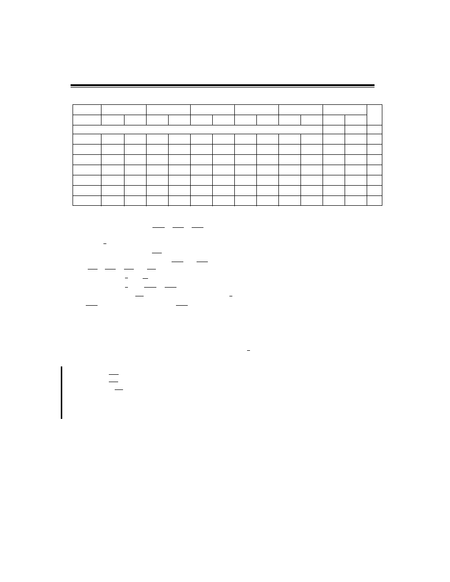
Table 3-3b (con’t): AC Characteristics (TA = 0 to 70°C, VDD = +5.0V ± 5%, VSS = 0V)
Notes:
1)
All input transition times assumed <5ns, except clock which is <3ns (for 25 and 33MHz timing).
2)
The appropriate input ag (
,
) goes active LOW after 1 CLK
↓ +30ns from the writing of a “Load” or
“Start” command.
3)
When S/S goes inactive (LOW) in Direct Control Mode, the ag associated with the Input Port will turn off.
4)
Direct Control Mode only (
must be LOW for one falling edge during a read/write cycle).
5)
In Cipher Feedback, the Port Flag (
or
) will go inactive following the leading edge of the rst data strobe
(
,
, or
), in all other modes and operations, the ags go inactive on the eighth data strobe.
6)
Do not change K/D until
is inactive (HIGH).
7)
Do not change E/D until
(
) is inactive (HIGH).
8)
In Cipher Feedback,
must be inactive (HIGH) before S/S goes inactive (LOW).
9)
must go active (LOW) before
goes active (LOW).
10) tWL is the clock width LOW (number t2).
11) tC is the clock cycle time (number t3).
12) All output timing specications reect the following: High output >1.5V, Low output <1.5V.
13) All output timings assume CLOAD = 50pF.
14) When operating in Direct Control Mode, you must ensure that the K/D input is valid one clock cycle before you begin to load
the key, or perform any data operations with the device.
15) Timing numbers for parameter t49 with CLOAD = 25 pF are shown below for a 33 MHz device:
For CA95C68:
LOW to Read Data VALID (Read Access Time): 23.5 ns
For CA95C18:
LOW to Read Data VALID (Read Access Time): 23.5 ns
For CA95C68/18:
LOW to Read Data VALID (Read Access Time): 19 ns
16) These input signals must be externally synchronized to the CA95C09’s clock. As a result, there is less timing margin as the
frequency increases (ie: @ 33 MHz). Designers should review these timing parameters early on in the design cycle to ensure
that their interface logic to the CA95C09/18/68 will be able to meet these timing requirements.
Number
5 MHz Limits
10 MHz Limits
16 MHz Limits
20 MHz Limits
25 MHz Limits
33 MHz Limits
Unit
Min
Max
Min
Max
Min
Max
Min
Max
Min
Max
Min
Max
Auxiliary Port Key Entry
t61
80
–
40
–
30
–
20
–
20
–
15
–
ns
t62
5tC-20
5
tC-20
5
tC-20
5
tC-20
5
tC-20
-12
tC-20
ns
t63
30
–
20
–
15
–
10
–
10
–
8
–
ns
t64
40
–20
–
15
–10
–5–3–ns
t65
20
–20
–
15
–15
–5–3–ns
t66
–
75
–
50
–
40
–
35
–
30
–
25
ns
t67
–
75
–
50
–
40
–
35
–
30
–
20
ns
MFLG
SFLG
AFLG
MCS
MFLG
SFLG
MRD
MWR
MDS
SDS
CP
MFLG
SFLG
BSY
AFLG
ASTB
MRD
MDS
SDS
相关PDF资料 |
PDF描述 |
|---|---|
| CA95C09-16CT | TELECOM, DATA ENCRYPTION CIRCUIT, PQFP44 |
| CA95C09-20CT | TELECOM, DATA ENCRYPTION CIRCUIT, PQFP44 |
| CA95C09-25CT | TELECOM, DATA ENCRYPTION CIRCUIT, PQFP44 |
| CA95C09-33CT | TELECOM, DATA ENCRYPTION CIRCUIT, PQFP44 |
| CA95C09-5CT | TELECOM, DATA ENCRYPTION CIRCUIT, PQFP44 |
相关代理商/技术参数 |
参数描述 |
|---|---|
| CA96 | 制造商:Datak Corporation 功能描述: |
| CA9623-000 | 功能描述:CABLE RoHS:是 类别:线缆,导线 >> 同轴 系列:- 产品培训模块:General Cable 标准包装:1 系列:- 缆线类型:细电缆网 - 耐热阻燃型 缆线组:RG-58 线规:20 AWG(0.62mm²) 线束:19 股 / 32 AWG 套管类型:聚氯乙烯(PVC) 套管直径:0.186"(4.72mm) 屏蔽类型:箔,编织线 阻抗:50 欧姆 长度:100' (30.5m) 颜色:灰 使用:网络 特点:- 导线材料:铜,镀锡 电介质材料:多孔(泡沫)聚乙烯(多孔 FPE) 电介质直径:0.100"(2.54mm) 屏蔽材料:Flexfoil?; 铜,镀锡 屏蔽覆盖范围:100%,81% VoP,传输速度:80 工作温度:- 其它名称:C5779-100 |
| CA9652-000 | 制造商:TE Connectivity 功能描述:- Bulk |
| CA9681-000 | 制造商:TE Connectivity 功能描述:CA9681-000 |
| CA9809-000 | 制造商:TE Connectivity 功能描述:Heat Shrink Molded Boot 制造商:TE Connectivity 功能描述:222K142-25-CS-2101-0 - Bulk |
发布紧急采购,3分钟左右您将得到回复。