- 您现在的位置:买卖IC网 > PDF目录20400 > DC1663A (Linear Technology)DEMO BOARD LTM4628 PDF资料下载
参数资料
| 型号: | DC1663A |
| 厂商: | Linear Technology |
| 文件页数: | 11/36页 |
| 文件大小: | 0K |
| 描述: | DEMO BOARD LTM4628 |
| 软件下载: | LTM4628 Spice Model |
| 设计资源: | LTM4628 Gerber Files DC1663A Design Files |
| 标准包装: | 1 |
| 系列: | µModule® |
| 主要目的: | DC/DC,步降 |
| 输出及类型: | 2,非隔离 |
| 输出电压: | 1.2V,1.5V |
| 电流 - 输出: | 8A,8A |
| 输入电压: | 4.5 ~ 26.5 V |
| 稳压器拓扑结构: | 降压 |
| 频率 - 开关: | 400kHz |
| 板类型: | 完全填充 |
| 已供物品: | 板 |
| 已用 IC / 零件: | LTM4628 |
第1页第2页第3页第4页第5页第6页第7页第8页第9页第10页当前第11页第12页第13页第14页第15页第16页第17页第18页第19页第20页第21页第22页第23页第24页第25页第26页第27页第28页第29页第30页第31页第32页第33页第34页第35页第36页
�� �
�
�LTM4628�
�APPLICATIONS� INFORMATION�
�V� OUT� =� 0.6V� ?�
�LTM4628�
�V� OUT1�
�V� OUTS1�
�TRACK1�
�V� FB2�
�V� OUT1�
�COMP1�
�The typical LTM4628 application circuit is shown in�
�Figure� 28.� External� component� selection� is� primarily�
�determined� by� the� maximum� load� current� and� output�
�voltage.� Refer� to� Table� 4� for� specific� external� capacitor�
�requirements� for� particular� applications.�
�V� IN� to� V� OUT� Step-Down� Ratios�
�There� are� restrictions� in� the� maximum� V� IN� and� V� OUT� step-�
�down� ratio� that� can� be� achieved� for� a� given� input� voltage.�
�Each� output� of� the� LTM4628� is� capable� of� 98%� duty� cycle,�
�but� the� V� IN� to� V� OUT� minimum� dropout� is� still� shown� as� a�
�function� of� its� load� current� and� will� limit� output� current�
�capability� related� to� high� duty� cycle� on� the� top� side� switch.�
�Minimum� on-time� t� ON(MIN)� is� another� consideration� in�
�operating� at� a� specified� duty� cycle� while� operating� at� a�
�certain� frequency� due� to� the� fact� that� t� ON(MIN)� <� D/f� SW� ,�
�where� D� is� duty� cycle� and� f� SW� is� the� switching� frequency.�
�t� ON(MIN)� is� specified� in� the� electrical� parameters� as� 90ns.�
�Output� Voltage� Programming�
�The� PWM� controller� has� an� internal� 0.6V� reference� voltage.�
�As� shown� in� the� Block� Diagram,� a� 60.4k?� internal� feedback�
�resistor� connects� between� the� V� OUTS1� to� V� FB1� and� V� OUTS2�
�to� V� FB2� .� It� is� very� important� that� these� pins� be� connected�
�to� their� respective� outputs� for� proper� feedback� regulation.�
�Overvoltage� can� occur� if� these� V� OUTS1� and� V� OUTS2� pins� are�
�left� floating� when� used� as� individual� regulators,� or� at� least�
�one� of� them� is� used� in� paralleled� regulators.� The� output�
�voltage� will� default� to� 0.6V� with� no� feedback� resistor� on�
�either� V� FB1� or� V� FB2� .� Adding� a� resistor� R� FB� from� V� FB� pin� to�
�GND� programs� the� output� voltage:�
�60.4k� +� R� FB�
�R� FB�
�In� parallel� operation� the� V� FB� pins� have� an� I� FB� current� of�
�20nA� maximum� each� channel.� To� reduce� output� voltage�
�error� due� to� this� current,� an� additional� V� OUTS� pin� can� be�
�tied� to� V� OUT� ,� and� an� additional� R� FB� resistor� can� be� used�
�to� lower� the� total� Thevenin� equivalent� resistance� seen� by�
�this� current.� For� example� in� Figure� 2,� the� total� Thevenin�
�equivalent� resistance� of� the� V� FB� pin� is� (60.4k� //� R� FB� ),� which�
�is� 30.2k� where� R� FB� is� equal� to� 60.4k� for� a� 1.2V� output.�
�Four� phases� connected� in� parallel� equates� to� a� worse� case�
�feedback� current� of� 4� ?� I� FB� equals� 80nA� maximum.� The� volt-�
�age� error� is� 80nA� ?� 30.2k� =� 2.4mV.� If� V� OUTS2� is� connected�
�as� shown� in� Figure� 2� to� V� OUT� ,� and� another� 60.4k� resistor� is�
�connected� from� V� FB2� to� ground,� then� the� voltage� error� is�
�reduced� to� 1.2mV.� If� the� voltage� error� is� acceptable� then�
�no� additional� connections� are� necessary.� The� onboard�
�60.4k� resistor� is� 0.5%� accurate� and� the� V� FB� resistor� can�
�be� chosen� by� the� user� to� be� as� accurate� as� needed.�
�All� COMP� pins� are� tied� together� for� current� sharing� between�
�the� phases.� The� TRACK� pins� can� be� tied� together� and� a� single�
�soft-start� capacitor� can� be� used� to� soft-start� the� regula-�
�tor.� The� soft-start� equation� will� need� to� have� the� soft-start�
�current� parameter� increased� by� the� number� of� paralleled�
�channels.� See� the� Output� Voltage� Tracking� section.�
�4� PARALLELED� OUTPUTS�
�COMP1� FOR� 1.2V� AT� 32A�
�COMP2� V� OUT2�
�60.4k�
�V� OUTS2�
�OPTIONAL� CONNECTION�
�V� FB1�
�60.4k�
�TRACK2�
�OPTIONAL�
�R� FB�
�60.4k�
�LTM4628�
�Table� 1.� V� FB� R� esistor� Table� vs� Various� Output� Voltages�
�V� OUT� 0.6V� 1.0V� 1.2V� 1.5V� 1.8V� 2.5V� 3.3V�
�R� FB� Open� 90.9k� 60.4k� 40.2k� 30.2k� 19.1k� 13.3k�
�5.0V�
�8.25k�
�COMP2�
�60.4k�
�V� OUT2�
�V� OUTS1�
�V� OUTS2�
�V� FB1�
�USED� TO� LOWER� TOTAL�
�THEVENIN� EQUIVALENT� TO�
�LOWER� I� FB� VOLTAGE� ERROR�
�TRACK1�
�V� FB2�
�R� FB�
�60.4k�
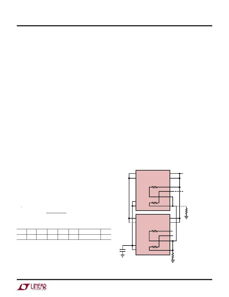
�Forparalleloperationofmultiplechannelsthesamefeed-�
�back� setting� resistor� can� be� used� for� the� parallel� design.�
�This� is� done� by� connecting� the� V� OUTS1� to� the� output� as�
�shown� in� Figure� 2,� thus� tying� one� of� the� internal� 60.4k�
�resistors� to� the� output.� All� of� the� V� FB� pins� tie� together� with�
�one� programming� resistor� as� shown� in� Figure� 2.�
�0.1μF�
�60.4k�
�TRACK2�
�4628� F02�
�Figure� 2.� 4-Phase� Parallel� Configurations�
�4628fe�
�For� more� information� www.linear.com/LTM4628�
�11�
�相关PDF资料 |
PDF描述 |
|---|---|
| IFSC1008ABER220M01 | INDUCTOR POWER 22UH 0.5A SMD |
| GSC10DRYI | CONN EDGECARD 20POS DIP .100 SLD |
| AT24C08B-TH-T | IC EEPROM 8KBIT 1MHZ 8TSSOP |
| T95Z226K016LSAL | CAP TANT 22UF 16V 10% 2910 |
| 346-080-540-202 | CARDEDGE 80POS DUAL .125 GREEN |
相关代理商/技术参数 |
参数描述 |
|---|---|
| DC1666A | 功能描述:BOARD DEMO LED DRIVER LT3791 RoHS:否 类别:编程器,开发系统 >> 评估板 - LED 驱动器 系列:- 标准包装:1 系列:PowerWise® 电流 - 输出 / 通道:20mA 输出及类型:1,非隔离 输出电压:17V 特点:可调光 输入电压:2.7 ~ 5.5 V 已供物品:板 已用 IC / 零件:LM3508 相关产品:LM3508TLX-ND - IC LED DRVR WHT BCKLGT 9USMDLM3508TLDKR-ND - IC LED DRVR WHT BCKLGT 9MICROSMDLM3508TLCT-ND - IC LED DRVR WHT BCKLGT 9MICROSMDLM3508TLTR-ND - IC LED DRVR WHT BCKLGT 9MICROSMD |
| DC1667 | 制造商:INTRONICS 制造商全称:INTRONICS 功能描述:15 Watt Triple Output DC-DC Converters |
| DC1668 | 制造商:INTRONICS 制造商全称:INTRONICS 功能描述:15 Watt Triple Output DC-DC Converters |
| DC1669 | 制造商:INTRONICS 制造商全称:INTRONICS 功能描述:15 Watt Triple Output DC-DC Converters |
| DC1669A | 功能描述:BOARD EVAL LTM4627 RoHS:否 类别:编程器,开发系统 >> 评估板 - DC/DC 与 AC/DC(离线)SMPS 系列:LTM®, uModule® 标准包装:1 系列:- 主要目的:DC/DC,步降 输出及类型:1,非隔离 功率 - 输出:- 输出电压:3.3V 电流 - 输出:3A 输入电压:4.5 V ~ 28 V 稳压器拓扑结构:降压 频率 - 开关:250kHz 板类型:完全填充 已供物品:板 已用 IC / 零件:L7981 其它名称:497-12113STEVAL-ISA094V1-ND |
发布紧急采购,3分钟左右您将得到回复。