- 您现在的位置:买卖IC网 > PDF目录171067 > DDP3315CQA (MICRONAS SEMICONDUCTOR HOLDING AG) SPECIALTY CONSUMER CIRCUIT, PQFP80 PDF资料下载
参数资料
| 型号: | DDP3315CQA |
| 厂商: | MICRONAS SEMICONDUCTOR HOLDING AG |
| 元件分类: | 消费家电 |
| 英文描述: | SPECIALTY CONSUMER CIRCUIT, PQFP80 |
| 封装: | PLASTIC, QFP-80 |
| 文件页数: | 56/62页 |
| 文件大小: | 1746K |
| 代理商: | DDP3315CQA |
第1页第2页第3页第4页第5页第6页第7页第8页第9页第10页第11页第12页第13页第14页第15页第16页第17页第18页第19页第20页第21页第22页第23页第24页第25页第26页第27页第28页第29页第30页第31页第32页第33页第34页第35页第36页第37页第38页第39页第40页第41页第42页第43页第44页第45页第46页第47页第48页第49页第50页第51页第52页第53页第54页第55页当前第56页第57页第58页第59页第60页第61页第62页
ADVANCE INFORMATION
6
Micronas
2. Functional Description
2.1. Display Part
The display part converts the digital YCrCb to analog
lation converts the digital input signal to YCrCb 4:2:2
standard format. The 4:2:2 YCrCb signal is processed
by the horizontal scaler. In the luminance processing
path, contrast and brightness adjustments and a vari-
ety of features, such as black level expander and luma
sharpness enhancer, are provided. In the chrominance
path, the CrCb signals are converted to 4:4:4 format
and filtered by a color transient improvement circuit.
The YCrCb signals are converted by a programmable
matrix to RGB color space.
2.1.1. Digital Input Interface
The digital input interface supports
– 16 bit 4:2:2 YCrCb with separate H/V-syncs and
clock (ITU-R-601 format)
– 12 bit 4:1:1 YCrCb with separate H/V-syncs and
clock (ITU-R-601 format)
– 8 bit 4:2:2 YCrCb multiplexed with encoded or sepa-
rate H/V-syncs and clock (ITU-R-656 format)
The data inputs Y0...Y7 and C0...C7 are clocked with
the external clock LLC2. The clock frequency is select-
able between 27 or 32 MHz for 12 and 16 bit data
input and 54 MHz for 8 bit data input. The horizontal
sync pulse at the HS pin should be an active video sig-
nal, which is not vertically blanked.
A clock generator converts the different external line
locked clock rates to a common internal sample rate of
approximately 40.5 MHz, in order to provide a fix
bandwidth for all digital filters. Therefore the input data
is sample rate converted to the common processing
frequency by the horizontal scaler.
2.1.2. Chroma Input
The chroma input signal can either be YCrCb in 4:1:1
or in 4:2:2 format. For the digital signal processing the
time-multiplexed chroma samples will be demulti-
plexed, synchronized with the signal at the HS Pin.
The input formatter accepts either two’s complement
or binary offset code. Also the delay can be adjusted
within a range of ±2 input clocks relative to the luma
signal; this doesn’t effect the chroma multiplex.
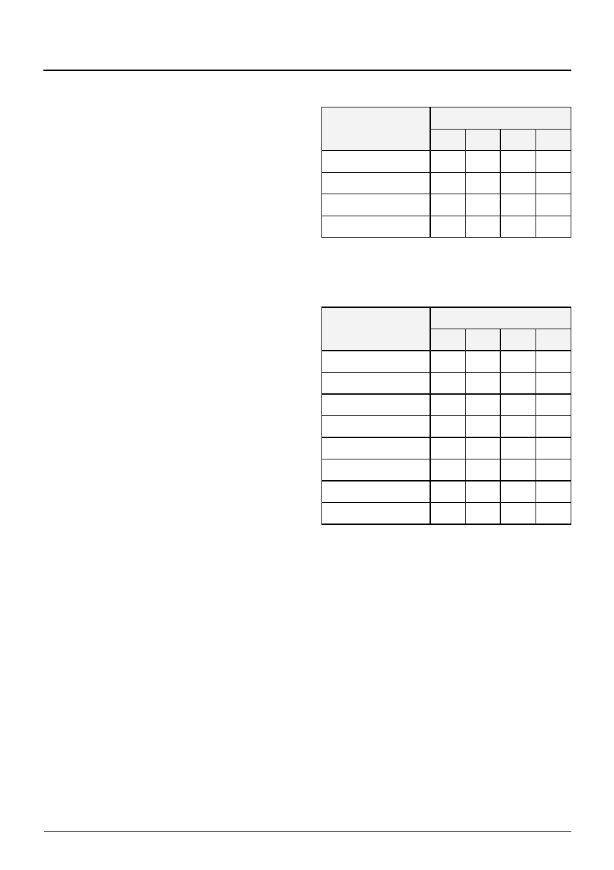
Note: Cx
y; x = pixel number; y = bit number
Table 2–1: 4:1:1 chroma format
Pin Name
Pixel Number
1
2
3
4
C7
Cb1
7
Cb1
5
Cb1
3
Cb1
1
C6
Cb1
6
Cb1
4
Cb1
2
Cb1
0
C5
Cr1
7
Cr1
5
Cr1
3
Cr1
1
C4
Cr1
6
Cr1
4
Cr1
2
Cr1
0
Table 2–2: 4:2:2 chroma format
Pin Name
Pixel Number
1
2
3
4
C7
Cb1
7
Cr1
7
Cb3
7
Cr3
7
C6
Cb1
6
Cr1
6
Cb3
6
Cr3
6
C5
Cb1
5
Cr1
5
Cb3
5
Cr3
5
C4
Cb1
4
Cr1
4
Cb3
4
Cr3
4
C3
Cb1
3
Cr1
3
Cb3
3
Cr3
3
C2
Cb1
2
Cr1
2
Cb3
2
Cr3
2
C1
Cb1
1
Cr1
1
Cb3
1
Cr3
1
C0
Cb1
0
Cr1
0
Cb3
0
Cr3
0
相关PDF资料 |
PDF描述 |
|---|---|
| DDQ24W7P043A00LF | 24 CONTACT(S), MALE, D SUBMINIATURE CONNECTOR, SOLDER |
| DDQ24W7PA00LF | 24 CONTACT(S), MALE, D SUBMINIATURE CONNECTOR, SOLDER |
| DDQ36W4P043A00LF | 36 CONTACT(S), MALE, D SUBMINIATURE CONNECTOR, SOLDER |
| DDQ36W4PA00LF | 36 CONTACT(S), MALE, D SUBMINIATURE CONNECTOR, SOLDER |
| DDQ47W1P043A00LF | 47 CONTACT(S), MALE, D SUBMINIATURE CONNECTOR, SOLDER |
相关代理商/技术参数 |
参数描述 |
|---|---|
| DDP-37CT | 制造商:Pan Pacific 功能描述: |
| DDP400-P1 | 制造商:CCM Assembly & Manufacturing 功能描述:AC Input Cable for ROAL DDP400 series, Bulk |
| DDP400-P4 | 制造商:CCM Assembly & Manufacturing 功能描述:DC Output Cable for ROAL DDP400 series, Bulk |
| DDP400-P6 | 制造商:CCM Assembly & Manufacturing 功能描述:Signal Cable for ROAL DDP400 series, Bulk |
| DDP400-US12-FF | 制造商:ROAL Electronics 功能描述:AC/DC 400W 12V Single Output Enclosed Front Fan, Bulk |
发布紧急采购,3分钟左右您将得到回复。