参数资料
| 型号: | DS1863K |
| 厂商: | Maxim Integrated Products |
| 文件页数: | 14/62页 |
| 文件大小: | 0K |
| 描述: | KIT EVAL FOR DS1863 |
| 产品培训模块: | Lead (SnPb) Finish for COTS Obsolescence Mitigation Program |
| 标准包装: | 1 |
| 主要目的: | 电信,无源光学网络(PON) |
| 已用 IC / 零件: | DS1863 |
第1页第2页第3页第4页第5页第6页第7页第8页第9页第10页第11页第12页第13页当前第14页第15页第16页第17页第18页第19页第20页第21页第22页第23页第24页第25页第26页第27页第28页第29页第30页第31页第32页第33页第34页第35页第36页第37页第38页第39页第40页第41页第42页第43页第44页第45页第46页第47页第48页第49页第50页第51页第52页第53页第54页第55页第56页第57页第58页第59页第60页第61页第62页
�� �
�
�Burst-Mode� PON� Controller�
�With� Integrated� Monitoring�
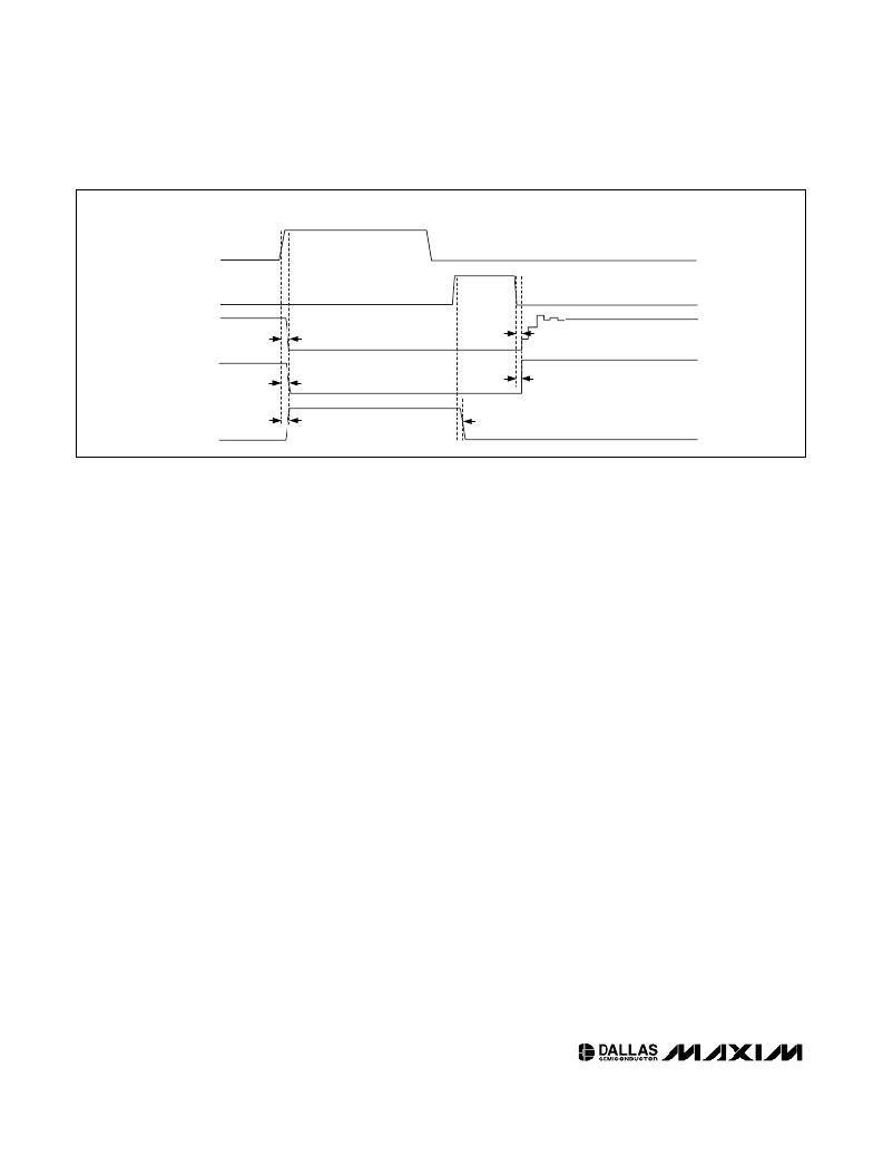
�FETG/OUTPUT� DISABLE� TIMING� (FAULT� CONDITION� DETECTED)�
�DETECTION� OF�
�FETG� FAULT�
�TX-D�
�I� BIAS�
�I� MOD�
�FETG�
�t� OFF�
�t� OFF�
�t� FETG:ON�
�t� ON�
�t� ON�
�t� FETG:OFF�
�Figure� 6.� FETG/Modulation� and� Bias� Timing� (Fault� Condition� Detected).�
�higher� level� is� an� Analog� POR� (V� POA� ).� At� start� up,�
�before� the� supply� voltage� rises� above� V� POA� ,� the� out-�
�puts� are� disabled� (FETG� and� BIAS� outputs� are� high�
�impedance,� MOD� is� low),� all� SRAM� outputs� are� low�
�(including� Shadowed� EEPROM),� and� all� analog� circuit-�
�ry� is� disabled.� When� V� CC� reaches� V� POA� ,� the� SEE� is�
�recalled,� and� the� analog� circuitry� is� enabled.� While�
�V� CC� remains� above� V� POA� ,� the� device� is� in� its� normal�
�operating� state,� and� it� responds� based� on� its� non-�
�volatile� configuration.� If� during� operation� V� CC� falls�
�below� V� POA� ,� but� is� still� above� V� POD� ,� then� the� SRAM�
�will� retain� the� SEE� settings� from� the� first� SEE� recall,� but�
�the� device� analog� will� be� shut� down� and� the� outputs�
�disabled.� FETG� will� be� driven� to� its� alarm� state� defined�
�by� the� FETG� DIR� bit� (Table� 02h,� Register� 89h).� If� the�
�supply� voltage� recovers� back� above� V� POA� ,� then� the�
�device� will� immediately� resume� normal� functioning.� If�
�the� supply� voltage� falls� below� V� POD� ,� then� the� device�
�SRAM� will� be� placed� in� its� default� state� and� another�
�SEE� recall� will� be� required� to� reload� the� nonvolatile� set-�
�tings.� The� EEPROM� recall� will� occur� the� next� time� V� CC�
�next� exceeds� V� POA� .� Figure� 7� shows� the� sequence� of�
�events� as� the� voltage� varies.�
�Any� time� V� CC� is� above� V� POD� ,� the� I� 2� C� interface� can� be�
�used� to� determine� if� V� CC� is� below� the� V� POA� level.� This�
�is� accomplished� by� checking� the� RDYB� bit� in� the� Status�
�(6Eh)� byte.� RDYB� is� set� when� V� CC� is� below� V� POA� ;� when�
�V� CC� rises� above� V� POA� RDYB� is� timed� (within� 500μs)� to�
�go� to� 0,� at� which� point� the� part� is� fully� functional.�
�For� all� Device� Addresses� sourced� from� EEPROM� (Byte�
�8Ch,� Table� 01h� in� memory)� the� default� Device� Address�
�is� A2h� until� V� CC� exceeds� V� POA� allowing� the� device�
�address� to� be� recalled� from� the� EEPROM.�
�Power-On� Analog� (POA)�
�POA� holds� the� DS1863� in� reset� until� V� CC� is� at� a� suitable�
�level� (V� CC� >� V� POA� )� for� the� part� to� accurately� measure�
�with� its� ADC� and� compare� analog� signals� with� its� quick-�
�trip� monitors.� Because� V� CC� cannot� be� measured� by� the�
�ADC� when� V� CC� is� less� than� V� POA� ,� POA� also� asserts� the�
�V� CC� low� alarm,� which� must� be� cleared� by� a� V� CC� ADC�
�conversion� that� is� greater� than� the� customer� programma-�
�ble� V� CC� low� ADC� limit.� This� prevents� the� TX-F� and� FETG�
�outputs� from� glitching� during� a� slow� power� up.� The� TX-F�
�and� FETG� output� will� not� latch� until� there� is� a� conversion�
�above� V� CC� low� limit.�
�The� POA� alarm� is� non-maskable.� The� TX-F,� and� FETG�
�outputs� shuts� off� any� time� V� CC� is� below� V� POA� .� See� Low�
�Voltage� Operation� section� for� more� information.�
�14�
�____________________________________________________________________�
�相关PDF资料 |
PDF描述 |
|---|---|
| DS1864K | KIT EVAL FOR DS1864 |
| DS21349DK | KIT DESIGN FOR DS21349 |
| DS21352DK | KIT DESIGN FOR DS21352 |
| DS21354DK | KIT DESIGN FOR DS21354 |
| DS21458DK | KIT DESIGN FOR G511DS21458 |
相关代理商/技术参数 |
参数描述 |
|---|---|
| DS1863T+ | 制造商:Maxim Integrated Products 功能描述:- Rail/Tube |
| DS1864 | 制造商:DALLAS 制造商全称:Dallas Semiconductor 功能描述:SFP Laser Controller and Diagnostic IC |
| DS1864K | 功能描述:电源管理IC开发工具 RoHS:否 制造商:Maxim Integrated 产品:Evaluation Kits 类型:Battery Management 工具用于评估:MAX17710GB 输入电压: 输出电压:1.8 V |
| DS1864T | 制造商:Maxim Integrated Products 功能描述:DUAL TMP CTRL DAC+MONITORS,QFN - Rail/Tube |
| DS1864T+ | 功能描述:激光驱动器 SFP Laser Controller & Diagnostic IC RoHS:否 制造商:Micrel 数据速率:4.25 Gbps 工作电源电压:3 V to 3.6 V 电源电流:80 mA 最大工作温度:+ 85 C 封装 / 箱体:QFN-16 封装:Tube |
发布紧急采购,3分钟左右您将得到回复。