参数资料
| 型号: | DS1863K |
| 厂商: | Maxim Integrated Products |
| 文件页数: | 18/62页 |
| 文件大小: | 0K |
| 描述: | KIT EVAL FOR DS1863 |
| 产品培训模块: | Lead (SnPb) Finish for COTS Obsolescence Mitigation Program |
| 标准包装: | 1 |
| 主要目的: | 电信,无源光学网络(PON) |
| 已用 IC / 零件: | DS1863 |
第1页第2页第3页第4页第5页第6页第7页第8页第9页第10页第11页第12页第13页第14页第15页第16页第17页当前第18页第19页第20页第21页第22页第23页第24页第25页第26页第27页第28页第29页第30页第31页第32页第33页第34页第35页第36页第37页第38页第39页第40页第41页第42页第43页第44页第45页第46页第47页第48页第49页第50页第51页第52页第53页第54页第55页第56页第57页第58页第59页第60页第61页第62页
�� �
�
�Burst-Mode� PON� Controller�
�With� Integrated� Monitoring�
�Acknowledge� Polling:� Any� time� an� EEPROM� location�
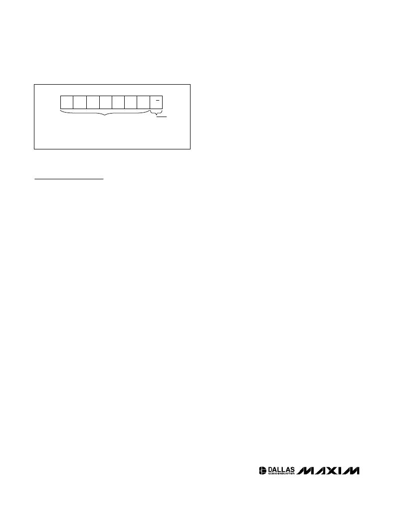
�MSB�
�LSB�
�is� written,� the� DS1863� requires� the� EEPROM� write� time�
�1�
�0�
�1�
�0�
�0�
�0�
�1�
�R/W�
�(t� W� )� after� the� STOP� condition� to� write� the� contents� of�
�the� byte� of� data� to� EEPROM.� During� the� EEPROM� write�
�SLAVE�
�ADDRESS*�
�READ/WRITE�
�BIT�
�time,� the� device� will� not� acknowledge� its� slave� address�
�because� it� is� busy.� It� is� possible� to� take� advantage� of�
�that� phenomenon� by� repeatedly� addressing� the�
�THE� DEFAULT� SLAVE� ADDRESS� IS� SHOWN,� HOWEVER� IT� CAN� BE� CHANGED�
�USING� THE� DEVICE� ADDRESS� BYTE� (TABLE� 02h,� BYTE� 8Ch).,� AND� ASEL� BIT.�
�Figure� 10.� DS1863� Slave� Address� Byte� (Default)�
�I� 2� C� Communication�
�Writing� a� Single� Byte� to� a� Slave:� The� master� must�
�generate� a� START� condition,� write� the� slave� address�
�byte� (R/� W� =� 0),� write� the� byte� of� data,� and� generate� a�
�STOP� condition.� The� master� must� read� the� slave� ’� s�
�acknowledgement� during� all� byte� write� operations.�
�Writing� Multiple� Bytes� to� a� Slave:� To� write� multiple�
�bytes� to� a� slave,� the� master� generates� a� start� condition,�
�writes� the� slave� address� byte� (R/� W� =� 0),� writes� the�
�memory� address,� writes� up� to� 8� data� bytes,� and� gener-�
�ates� a� stop� condition.� The� DS1863� writes� 1� to� 8� bytes� (1�
�page� or� row)� with� a� single� write� transaction.� This� is�
�internally� controlled� by� an� address� counter� that� allows�
�data� to� be� written� to� consecutive� addresses� without�
�transmitting� a� memory� address� before� each� data� byte� is�
�sent.� The� address� counter� limits� the� write� to� one� 8-byte�
�page� (one� row� of� the� memory� map).� Attempts� to� write� to�
�additional� pages� of� memory� without� sending� a� stop�
�condition� between� pages� results� in� the� address� counter�
�wrapping� around� to� the� beginning� of� the� present� row.�
�Example:� A� 3-byte� write� starts� at� address� 06h� and�
�writes� three� data� bytes� (11h,� 22h,� and� 33h)� to� three�
�“� consecutive� ”� addresses.� The� result� is� that� addresses�
�06h� and� 07h� would� contain� 11h� and� 22h,� respectively,�
�and� the� third� data� byte,� 33h,� would� be� written� to�
�address� 00h.�
�To� prevent� address� wrapping� from� occurring,� the� mas-�
�ter� must� send� a� stop� condition� at� the� end� of� the� page,�
�then� wait� for� the� bus-free� or� EEPROM-write� time� to�
�elapse.� Then� the� master� can� generate� a� new� start� con-�
�dition,� and� write� the� slave� address� byte� (R/� W� =� 0)� and�
�the� first� memory� address� of� the� next� memory� row�
�before� continuing� to� write� data.�
�DS1863,� which� allows� the� next� page� to� be� written� as�
�soon� as� the� DS1863� is� ready� to� receive� the� data.� The�
�alternative� to� acknowledge� polling� is� to� wait� for� a� maxi-�
�mum� period� of� t� W� to� elapse� before� attempting� to� write�
�again� to� the� device.�
�EEPROM� Write� Cycles:� When� EEPROM� writes� occur� to�
�the� memory,� the� DS1863� will� write� to� all� three� EEPROM�
�memory� locations,� even� if� only� a� single� byte� was� modi-�
�fied.� Because� all� three� bytes� are� written,� the� bytes� that�
�were� not� modified� during� the� write� transaction� are� still�
�subject� to� a� write� cycle.� This� can� result� in� all� three� bytes�
�being� worn� out� over� time� by� writing� a� single� byte� repeat-�
�edly.� The� DS1863� ’� s� EEPROM� write� cycles� are� specified� in�
�the� NV� Memory� Characteristics� table.� The� specification�
�shown� is� at� the� worst-case� temperature.� If� zero-crossing�
�detection� is� enabled,� EEPROM� write� cycles� cannot� begin�
�until� after� the� zero-crossing� detection� is� complete.�
�Reading� a� Single� Byte� from� a� Slave:� To� read� a� single�
�byte� from� the� slave,� the� master� generates� a� START� con-�
�dition,� writes� the� slave� address� byte� with� R/� W� =� 1,� reads�
�the� data� byte� with� a� NACK� to� indicate� the� end� of� the�
�transfer,� and� generates� a� STOP� condition.� When� a� single�
�byte� is� read,� it� will� always� be� the� Potentiometer� 0� value.�
�Reading� Multiple� Bytes� from� a� Slave:� The� read� oper-�
�ation� can� be� used� to� read� multiple� bytes� with� a� single�
�transfer.� When� reading� bytes� from� the� slave,� the� master�
�simply� ACKs� the� data� byte� if� it� desires� to� read� another�
�byte� before� terminating� the� transaction.� After� the� mas-�
�ter� reads� the� last� byte,� it� NACKs� to� indicate� the� end� of�
�the� transfer� and� generates� a� STOP� condition.� The� first�
�byte� read� will� be� the� Potentiometer� 0� Wiper� Setting.� The�
�next� byte� will� be� the� Potentiometer� 1� Wiper� Setting.� The�
�third� byte� is� the� Configuration� Register� byte.� If� an� ACK�
�is� issued� by� the� master� following� the� Configuration�
�Register� byte,� then� the� DS1863� will� send� the�
�Potentiometer� 0� Wiper� Setting� again.� This� round� robin�
�reading� will� occur� as� long� as� each� byte� read� is� followed�
�by� an� ACK� from� the� master.�
�18�
�____________________________________________________________________�
�相关PDF资料 |
PDF描述 |
|---|---|
| DS1864K | KIT EVAL FOR DS1864 |
| DS21349DK | KIT DESIGN FOR DS21349 |
| DS21352DK | KIT DESIGN FOR DS21352 |
| DS21354DK | KIT DESIGN FOR DS21354 |
| DS21458DK | KIT DESIGN FOR G511DS21458 |
相关代理商/技术参数 |
参数描述 |
|---|---|
| DS1863T+ | 制造商:Maxim Integrated Products 功能描述:- Rail/Tube |
| DS1864 | 制造商:DALLAS 制造商全称:Dallas Semiconductor 功能描述:SFP Laser Controller and Diagnostic IC |
| DS1864K | 功能描述:电源管理IC开发工具 RoHS:否 制造商:Maxim Integrated 产品:Evaluation Kits 类型:Battery Management 工具用于评估:MAX17710GB 输入电压: 输出电压:1.8 V |
| DS1864T | 制造商:Maxim Integrated Products 功能描述:DUAL TMP CTRL DAC+MONITORS,QFN - Rail/Tube |
| DS1864T+ | 功能描述:激光驱动器 SFP Laser Controller & Diagnostic IC RoHS:否 制造商:Micrel 数据速率:4.25 Gbps 工作电源电压:3 V to 3.6 V 电源电流:80 mA 最大工作温度:+ 85 C 封装 / 箱体:QFN-16 封装:Tube |
发布紧急采购,3分钟左右您将得到回复。