参数资料
| 型号: | DS1863K |
| 厂商: | Maxim Integrated Products |
| 文件页数: | 4/62页 |
| 文件大小: | 0K |
| 描述: | KIT EVAL FOR DS1863 |
| 产品培训模块: | Lead (SnPb) Finish for COTS Obsolescence Mitigation Program |
| 标准包装: | 1 |
| 主要目的: | 电信,无源光学网络(PON) |
| 已用 IC / 零件: | DS1863 |
第1页第2页第3页当前第4页第5页第6页第7页第8页第9页第10页第11页第12页第13页第14页第15页第16页第17页第18页第19页第20页第21页第22页第23页第24页第25页第26页第27页第28页第29页第30页第31页第32页第33页第34页第35页第36页第37页第38页第39页第40页第41页第42页第43页第44页第45页第46页第47页第48页第49页第50页第51页第52页第53页第54页第55页第56页第57页第58页第59页第60页第61页第62页
�� �
�
�Burst-Mode� PON� Controller�
�With� Integrated� Monitoring�
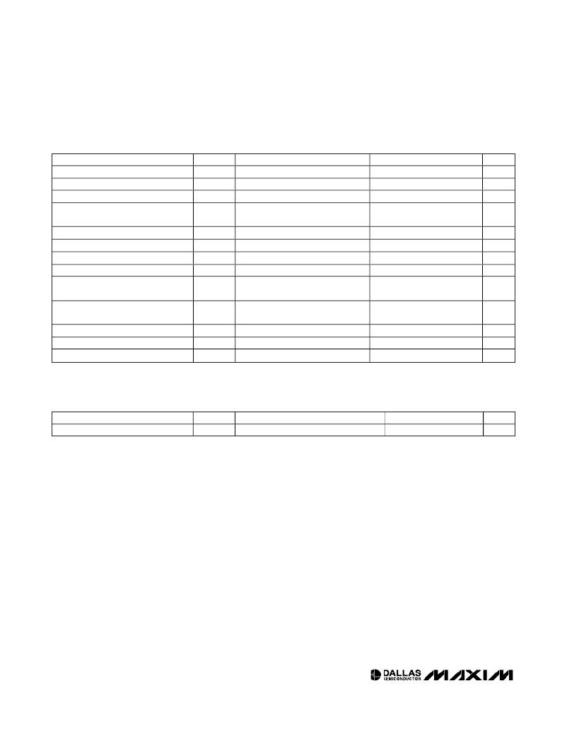
�I� 2� C� AC� ELECTRICAL� CHARACTERISTICS�
�(V� CC� =� +2.85V� to� +3.9V,� T� A� =� -40°C� to� +95°C,� unless� otherwise� noted,� see� Figure� 9.)�
�PARAMETER�
�SCL� Clock� Frequency�
�SYMBOL�
�f� SCL�
�(Note� 12)�
�CONDITIONS�
�MIN�
�0�
�TYP�
�MAX�
�400�
�UNITS�
�kHz�
�Clock� Pulse-Width� Low�
�Clock� Pulse-Width� High�
�Bus� Free� Time� Between� STOP� and�
�START� Condition�
�START� Hold� Time�
�START� Setup� Time�
�t� LOW�
�t� HIGH�
�t� BUF�
�t� HD:STA�
�t� SU:STA�
�1.3�
�0.6�
�1.3�
�0.6�
�0.6�
�μs�
�μs�
�μs�
�μs�
�μs�
�Data-In� Hold� Time�
�Data-In� Setup� Time�
�t� HD:DAT�
�t� SU:DAT�
�0�
�100�
�0.9�
�μs�
�ns�
�Rise� Time� of� Both� SDA� and�
�SCL� Signals�
�Fall� Time� of� Both� SDA� and�
�SCL� Signals�
�STOP� Setup� Time�
�Capacitive� Load� for� Each� Bus� Line�
�EEPROM� Write� Time�
�t� R�
�t� F�
�t� SU:STO�
�C� B�
�t� W�
�(Note� 13)�
�(Note� 13)�
�(Note� 13)�
�(Note� 14)�
�20� +� 0.1C� B�
�20� +� 0.1C� B�
�0.6�
�300�
�300�
�400�
�20�
�ns�
�ns�
�μs�
�pF�
�ms�
�NONVOLATILE� MEMORY� CHARACTERISTICS�
�(V� CC� =� +2.85V� to� +3.9V,� unless� otherwise� noted.)�
�PARAMETER�
�SYMBOL�
�CONDITIONS�
�MIN�
�TYP�
�MAX�
�UNITS�
�EEPROM� Write� Cycles�
�+70°C�
�50,000�
�Note� 1:�
�Note� 2:�
�Note� 3:�
�Note� 4:�
�Note� 5:�
�Note� 6:�
�Note� 7:�
�Note� 8:�
�Note� 9:�
�Note� 10:�
�Note� 11:�
�Note� 12:�
�Note� 13:�
�Note� 14:�
�All� voltages� are� referenced� to� ground.� Currents� into� the� IC� are� positive� and� out� of� the� IC� are� negative.�
�Digital� Inputs� are� at� rail.� FETG� is� disconnected� SDA� =� SCL� =� 1.�
�See� the� Safety� Shutdown� (FETG)� Output� section� for� details.�
�Eight� ranges� allow� the� full-scale� range� to� change� from� 625mV� to� 2.5V.�
�This� specification� applies� to� the� expected� full-scale� value� for� the� selected� range.� See� the� Comp� Ranging� byte� for� available�
�full-scale� ranges.�
�Eight� ranges� allow� the� full-scale� range� to� change� from� 312.5mV� to� 1.25V.�
�The� output� impedance� of� the� DS1863� is� proportional� to� its� scale� setting.� For� instance,� if� using� the� 1/2� scale,� the� output�
�impedance� would� be� 1.5k� Ω� .�
�This� specification� applies� to� the� expected� full-scale� value� for� the� selected� range.� See� the� Mod� Ranging� byte� for� available�
�full-scale� ranges.�
�See� the� APC/Quick-Trip� Sample� Timing� section� for� details.�
�Assuming� an� appropriate� initial� step� is� programmed� that� would� cause� the� power� to� exceed� the� APC� set� point� within� 4�
�steps,� the� bias� current� will� be� within� 1%� within� the� time� specified� by� the� binary� search� time.�
�Guaranteed� by� design.�
�I� 2� C� interface� timing� shown� is� for� fast-mode� (400kHz)� operation.� This� device� is� also� backward-compatible� with� I� 2� C� stan-�
�dard-mode� timing.�
�C� B� —total� capacitance� of� one� bus� line� in� picofarads.�
�EEPROM� write� begins� after� a� STOP� condition� occurs.�
�4�
�_____________________________________________________________________�
�相关PDF资料 |
PDF描述 |
|---|---|
| DS1864K | KIT EVAL FOR DS1864 |
| DS21349DK | KIT DESIGN FOR DS21349 |
| DS21352DK | KIT DESIGN FOR DS21352 |
| DS21354DK | KIT DESIGN FOR DS21354 |
| DS21458DK | KIT DESIGN FOR G511DS21458 |
相关代理商/技术参数 |
参数描述 |
|---|---|
| DS1863T+ | 制造商:Maxim Integrated Products 功能描述:- Rail/Tube |
| DS1864 | 制造商:DALLAS 制造商全称:Dallas Semiconductor 功能描述:SFP Laser Controller and Diagnostic IC |
| DS1864K | 功能描述:电源管理IC开发工具 RoHS:否 制造商:Maxim Integrated 产品:Evaluation Kits 类型:Battery Management 工具用于评估:MAX17710GB 输入电压: 输出电压:1.8 V |
| DS1864T | 制造商:Maxim Integrated Products 功能描述:DUAL TMP CTRL DAC+MONITORS,QFN - Rail/Tube |
| DS1864T+ | 功能描述:激光驱动器 SFP Laser Controller & Diagnostic IC RoHS:否 制造商:Micrel 数据速率:4.25 Gbps 工作电源电压:3 V to 3.6 V 电源电流:80 mA 最大工作温度:+ 85 C 封装 / 箱体:QFN-16 封装:Tube |
发布紧急采购,3分钟左右您将得到回复。