参数资料
| 型号: | DS1863K |
| 厂商: | Maxim Integrated Products |
| 文件页数: | 9/62页 |
| 文件大小: | 0K |
| 描述: | KIT EVAL FOR DS1863 |
| 产品培训模块: | Lead (SnPb) Finish for COTS Obsolescence Mitigation Program |
| 标准包装: | 1 |
| 主要目的: | 电信,无源光学网络(PON) |
| 已用 IC / 零件: | DS1863 |
第1页第2页第3页第4页第5页第6页第7页第8页当前第9页第10页第11页第12页第13页第14页第15页第16页第17页第18页第19页第20页第21页第22页第23页第24页第25页第26页第27页第28页第29页第30页第31页第32页第33页第34页第35页第36页第37页第38页第39页第40页第41页第42页第43页第44页第45页第46页第47页第48页第49页第50页第51页第52页第53页第54页第55页第56页第57页第58页第59页第60页第61页第62页
�� �
�
�Burst-Mode� PON� Controller�
�With� Integrated� Monitoring�
�Modulation� Control�
�The� MOD� voltage� is� controlled� using� an� internal� tem-�
�perature� indexed� Lookup� Table.�
�The� MOD� output� is� an� 8-bit� scaleable� voltage� output� that�
�interfaces� with� the� MAX3643� ’� s� VMSET� input.� An� external�
�resistor� to� ground� from� the� MAX3643� ’� s� MODSET� pin� sets�
�the� maximum� current� the� voltage� at� VMSET� input� can�
�produce� for� a� given� output� range.� This� resistor� value�
�should� be� chosen� to� produce� the� maximum� modulation�
�current� the� laser� type� requires� over� temperature.� The�
�modulation� LUT� can� be� programmed� in� 2� °� C� increments�
�over� the� -40� °� C� to� +102� °� C� range� to� provide� temperature�
�compensation� for� the� laser� ’� s� modulation.� The� modulation�
�DAC� ’� s� scaling� can� be� used� (with� APC� scaling)� to� imple-�
�ment� GPON� power� leveling� with� a� single� LUT� that� works�
�for� all� three� power� levels.�
�Ranging� of� the� MOD� DAC� is� possible� by� programming�
�a� single� byte� in� Table� 02h.�
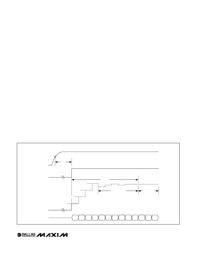
�BIAS� and� MOD� Output� During�
�Initial� Power-Up�
�On� power-up� the� modulation� and� bias� outputs� will�
�remain� off� until� V� CC� is� above� V� POA� ,� a� temperature� con-�
�version� has� been� completed,� and� if� the� V� CC� LO� ADC�
�alarm� is� enabled,� then� a� V� CC� conversion� above� the�
�customer� defined� V� CC� low� alarm� level� has� cleared� the�
�V� CC� low� alarm.� Once� all� of� these� conditions� are� satis-�
�POWER-UP� TIMING�
�V� POA�
�fied,� the� MOD� output� will� be� enabled� with� the� value�
�determined� by� the� temperature� conversion� and� the�
�modulation� LUT.�
�When� the� MOD� output� is� enabled� and� BEN� is� high,� the�
�I� BIAS� DAC� output� will� be� turned� on� to� a� value� equal� to�
�I� STEP� (see� above).� The� start-up� algorithm� checks� if� this�
�bias� current� causes� a� feedback� voltage� above� the� APC�
�set-point,� and� if� it� does� not� it� continues� increasing� the�
�I� BIAS� by� I� STEP� until� the� APC� set-point� is� exceeded.�
�When� the� APC� set� point� is� exceeded,� the� device� will�
�begin� a� binary� search� to� quickly� reach� the� bias� current�
�corresponding� to� the� proper� power� level.� After� the� bina-�
�ry� search� is� completed� the� APC� integrator� is� enabled,�
�and� single� LSB� steps� are� taken� to� tightly� control� the�
�average� power.�
�All� quick-trip� and� ADC� alarm� flags� are� masked� until� the�
�binary� search� is� completed.� However,� the� BIAS� MAX�
�alarm� is� monitored� during� this� time� to� prevent� the� bias�
�output� from� exceeding� MAX� IBIAS.� During� the� bias� cur-�
�rent� initialization,� the� bias� current� is� not� allowed� to�
�exceed� MAX� IBIAS.� If� this� occurs� during� the� I� STEP�
�sequence� then� the� binary� search� routine� is� enabled.� If�
�MAX� IBIAS� is� exceeded� during� the� binary� search,� then�
�the� next� smaller� step� is� activated.� I� STEP� or� binary� incre-�
�ments� that� would� cause� I� BIAS� to� exceed� MAX� IBIAS� are�
�not� taken.� Many� of� the� alarm� sources� are� likely� to� trip�
�V� CC�
�t� ON�
�MOD�
�VOLTAGE�
�t� SEARCH�
�4x� I� STEP�
�BIAS�
�CURRENT�
�3x� I� STEP�
�BINARY� SEARCH�
�APC�
�INTEGRATOR�
�ON�
�2x� I� STEP�
�I� STEP�
�BIAS�
�SAMPLE�
�1�
�2�
�3�
�4�
�5�
�6�
�7�
�8�
�9�
�10�
�11�
�12�
�13�
�Figure� 1.� DS1863� Power-Up.�
�_____________________________________________________________________�
�9�
�相关PDF资料 |
PDF描述 |
|---|---|
| DS1864K | KIT EVAL FOR DS1864 |
| DS21349DK | KIT DESIGN FOR DS21349 |
| DS21352DK | KIT DESIGN FOR DS21352 |
| DS21354DK | KIT DESIGN FOR DS21354 |
| DS21458DK | KIT DESIGN FOR G511DS21458 |
相关代理商/技术参数 |
参数描述 |
|---|---|
| DS1863T+ | 制造商:Maxim Integrated Products 功能描述:- Rail/Tube |
| DS1864 | 制造商:DALLAS 制造商全称:Dallas Semiconductor 功能描述:SFP Laser Controller and Diagnostic IC |
| DS1864K | 功能描述:电源管理IC开发工具 RoHS:否 制造商:Maxim Integrated 产品:Evaluation Kits 类型:Battery Management 工具用于评估:MAX17710GB 输入电压: 输出电压:1.8 V |
| DS1864T | 制造商:Maxim Integrated Products 功能描述:DUAL TMP CTRL DAC+MONITORS,QFN - Rail/Tube |
| DS1864T+ | 功能描述:激光驱动器 SFP Laser Controller & Diagnostic IC RoHS:否 制造商:Micrel 数据速率:4.25 Gbps 工作电源电压:3 V to 3.6 V 电源电流:80 mA 最大工作温度:+ 85 C 封装 / 箱体:QFN-16 封装:Tube |
发布紧急采购,3分钟左右您将得到回复。