- 您现在的位置:买卖IC网 > PDF目录11784 > DS80C400-FNY+ (Maxim Integrated Products)IC MCU 75MHZ 16MB HP 100-LQFP PDF资料下载
参数资料
| 型号: | DS80C400-FNY+ |
| 厂商: | Maxim Integrated Products |
| 文件页数: | 22/97页 |
| 文件大小: | 0K |
| 描述: | IC MCU 75MHZ 16MB HP 100-LQFP |
| 产品培训模块: | Lead (SnPb) Finish for COTS Obsolescence Mitigation Program |
| 标准包装: | 90 |
| 系列: | 80C |
| 核心处理器: | 8051 |
| 芯体尺寸: | 8-位 |
| 速度: | 75MHz |
| 连通性: | 1 线,CAN,EBI/EMI,以太网,SIO,UART/USART |
| 外围设备: | 电源故障复位,WDT |
| 输入/输出数: | 64 |
| 程序存储器容量: | 64KB(64K x 8) |
| 程序存储器类型: | ROM |
| RAM 容量: | 1K x 8 |
| 电压 - 电源 (Vcc/Vdd): | 1.62 V ~ 3.6 V |
| 振荡器型: | 外部 |
| 工作温度: | -40°C ~ 85°C |
| 封装/外壳: | 100-LQFP |
| 包装: | 托盘 |
| 配用: | DS80C400-KIT#-ND - EVAL KIT FOR DS80C400 |
| 其它名称: | DS80C400+FNY DS80C400+FNY+ DS80C400+FNY+-ND DS80C400+FNY-ND |
第1页第2页第3页第4页第5页第6页第7页第8页第9页第10页第11页第12页第13页第14页第15页第16页第17页第18页第19页第20页第21页当前第22页第23页第24页第25页第26页第27页第28页第29页第30页第31页第32页第33页第34页第35页第36页第37页第38页第39页第40页第41页第42页第43页第44页第45页第46页第47页第48页第49页第50页第51页第52页第53页第54页第55页第56页第57页第58页第59页第60页第61页第62页第63页第64页第65页第66页第67页第68页第69页第70页第71页第72页第73页第74页第75页第76页第77页第78页第79页第80页第81页第82页第83页第84页第85页第86页第87页第88页第89页第90页第91页第92页第93页第94页第95页第96页第97页
DS80C400 Network Microcontroller
29 of 97
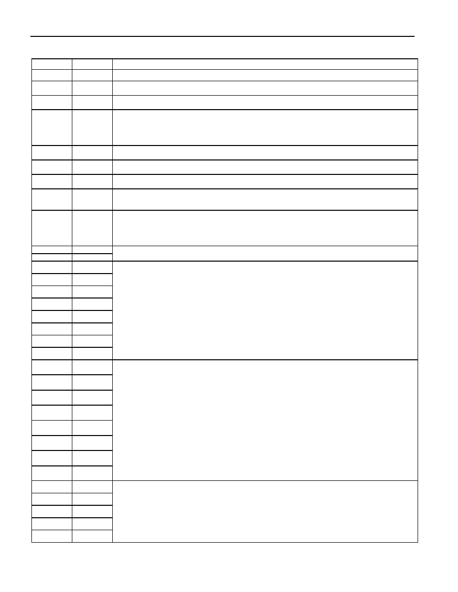
PIN DESCRIPTION
PIN
NAME
FUNCTION
70
VCC1
+1.8V Core Supply Voltage
12, 36, 62,
87
VCC3
+3.3V I/O Supply Voltage
13, 39, 63,
88
VSS
Digital Circuit Ground
68
ALE
Address Latch Enable, Output. When the MUX pin is low, this pin outputs a clock to latch the external address
LSB from the multiplexed address/data bus on Port 0. This signal is commonly connected to the latch enable of
an external transparent latch. ALE has a pulse width of 1.5 XTAL1 cycles and a period of four XTAL1 cycles.
When the MUX pin is high, the pin toggles continuously if the ALEOFF bit is cleared. ALE is forced high when
the device is in a reset condition or if the ALEOFF bit is set while the MUX pin is high.
67
PSEN
Program Store Enable, Output. This signal is the chip enable for external program or merged program/data
memory. PSEN provides an active-low pulse and is driven high when external memory is not being accessed.
69
EA
External Access Enable, Input. Connect to GND to use external program memory. Connect to VCC to use
internal ROM.
40
MUX
Multiplex/Demultiplex Select, Input. This pin selects if the address/data bus operates in multiplexed (MUX =
0) or demultiplexed (MUX = 1) mode. The MUX pin is sampled only on a power-on reset.
97
RST
Reset, Input. The RST input pin contains a Schmitt voltage input to recognize external active-high reset inputs.
The pin also employs an internal pulldown resistor to allow for a combination of wired-OR external-reset
sources. An RC circuit is not required for power-up, as the device provides this function internally.
98
RSTOL
Reset Output Low, Output. This active-low signal is asserted when the microcontroller has entered reset
through the RST pin; during crystal warm-up period following power-on or stop mode; during a watchdog timer
reset; during an oscillator failure (if OFDE = 1); whenever VCC1 ≤ VRST1 or VCC3 ≤ VRST3. When connecting the
DS80C400 to an external PHY, do not connect the RSTOL to the reset of the PHY. Doing so may disable the
Ethernet transmit.
37
XTAL2
XTAL1, XTAL2. Crystal oscillator pins support fundamental mode, parallel resonant, AT cut crystals. XTAL1 is
the input if an external clock source is used in place of a crystal. XTAL2 is the output of the crystal amplifier.
38
XTAL1
86
AD0/D0
AD0–7 (Port 0), I/O. When the MUX pin is connected low, Port 0 is the multiplexed address/data bus. While
ALE is high, the LSB of a memory address is presented. While ALE falls, the port transitions to a bidirectional
data bus. When the MUX pin is connected high, Port 0 functions as the bidirectional data bus. Port 0 cannot be
modified by software. The reset condition of Port 0 pins is high. No pullup resistors are needed.
Port
Alternate Function
P0.0
AD0/D0 (Address)/Data 0
P0.1
AD1/D1 (Address)/Data 1
P0.2
AD2/D2 (Address)/Data 2
P0.3
AD3/D3 (Address)/Data 3
P0.4
AD4/D4 (Address)/Data 4
P0.5
AD5/D5 (Address)/Data 5
P0.6
AD6/D6 (Address)/Data 6
P0.7
AD7/D7 (Address)/Data 7
85
AD1/D1
84
AD2/D2
83
AD3/D3
82
AD4/D4
81
AD5/D5
80
AD6/D6
79
AD7/D7
89
P1.0
Port 1, I/O. Port 1 can function as either an 8-bit, bidirectional I/O port or as an alternate interface for internal
resources. The reset condition of Port 1 is all bits at logic 1 through a weak pullup. The logic 1 state also serves
as an input mode, since external circuits writing to the port can override the weak pullup. When software clears
any port pin to 0, a strong pulldown is activated that remains on until either a 1 is written to the port pin or a
reset occurs. Writing a 1 after the port has been at 0 activates a strong transition driver, followed by a weaker
sustaining pullup. Once the momentary strong driver turns off, the port once again becomes the output (and
input) high state.
Port
Alternate Function
P1.0
T2 External I/O for Timer/Counter 2
P1.1
T2EX Timer/Counter 2 Capture/Reload Trigger
P1.2
RXD1 Serial Port 1 Receive
P1.3
TXD1 Serial Port 1 Transmit
P1.4
INT2 External Interrupt 2 (Positive Edge Detect)
P1.5
INT3
External Interrupt 3 (Negative Edge Detect)
P1.6
INT4 External Interrupt 4 (Positive Edge Detect)
P1.7
INT5
External Interrupt 5 (Negative Edge Detect)
90
P1.1
91
P1.2
92
P1.3
93
P1.4
94
P1.5
95
P1.6
96
P1.7
66
A8
A15–A8 (Port 2), Output. Port 2 serves as the MSB for external addressing. The port automatically asserts the
address MSB during external ROM and RAM access. Although the Port 2 SFR exists, the SFR value never
appears on the pins (due to memory access). Therefore, accessing the Port 2 SFR is only useful for MOVX A,
@Ri or MOVX @Ri, A instructions, which use the Port 2 SFR as the external address MSB.
Port
Alternate Function
P2.0
A8 Program/Data Memory Address 8
P2.1
A9 Program/Data Memory Address 9
65
A9
64
A10
61
A11
60
A12
相关PDF资料 |
PDF描述 |
|---|---|
| VE-B43-IX-F1 | CONVERTER MOD DC/DC 24V 75W |
| DS89C450-ENL+ | IC MCU FLASH 64KB 33MHZ 44-TQFP |
| VE-B43-IW-F3 | CONVERTER MOD DC/DC 24V 100W |
| DS89C450-MNL+ | IC MCU FLASH 64KB 33MHZ 40-DIP |
| VE-B43-IW-F2 | CONVERTER MOD DC/DC 24V 100W |
相关代理商/技术参数 |
参数描述 |
|---|---|
| DS80C400-FNY+ | 功能描述:8位微控制器 -MCU Network MCU RoHS:否 制造商:Silicon Labs 核心:8051 处理器系列:C8051F39x 数据总线宽度:8 bit 最大时钟频率:50 MHz 程序存储器大小:16 KB 数据 RAM 大小:1 KB 片上 ADC:Yes 工作电源电压:1.8 V to 3.6 V 工作温度范围:- 40 C to + 105 C 封装 / 箱体:QFN-20 安装风格:SMD/SMT |
| DS80C400-KIT | 功能描述:EVAL KIT FOR DS80C400 RoHS:否 类别:编程器,开发系统 >> 通用嵌入式开发板和套件(MCU、DSP、FPGA、CPLD等) 系列:- 产品培训模块:Blackfin® Processor Core Architecture Overview Blackfin® Device Drivers Blackfin® Optimizations for Performance and Power Consumption Blackfin® System Services 特色产品:Blackfin? BF50x Series Processors 标准包装:1 系列:Blackfin® 类型:DSP 适用于相关产品:ADSP-BF548 所含物品:板,软件,4x4 键盘,光学拨轮,QVGA 触摸屏 LCD 和 40G 硬盘 配用:ADZS-BFBLUET-EZEXT-ND - EZ-EXTENDER DAUGHTERBOARDADZS-BFLLCD-EZEXT-ND - BOARD EXT LANDSCAP LCD INTERFACE 相关产品:ADSP-BF542BBCZ-4A-ND - IC DSP 16BIT 400MHZ 400CSBGAADSP-BF544MBBCZ-5M-ND - IC DSP 16BIT 533MHZ MDDR 400CBGAADSP-BF542MBBCZ-5M-ND - IC DSP 16BIT 533MHZ MDDR 400CBGAADSP-BF542KBCZ-6A-ND - IC DSP 16BIT 600MHZ 400CSBGAADSP-BF547MBBCZ-5M-ND - IC DSP 16BIT 533MHZ MDDR 400CBGAADSP-BF548BBCZ-5A-ND - IC DSP 16BIT 533MHZ 400CSBGAADSP-BF547BBCZ-5A-ND - IC DSP 16BIT 533MHZ 400CSBGAADSP-BF544BBCZ-5A-ND - IC DSP 16BIT 533MHZ 400CSBGAADSP-BF542BBCZ-5A-ND - IC DSP 16BIT 533MHZ 400CSBGA |
| DS80C400-KIT# | 功能描述:开发板和工具包 - 8051 RoHS:否 制造商:Silicon Labs 产品:Development Kits 工具用于评估:C8051F960, Si7005 核心: 接口类型:USB 工作电源电压: |
| DS80C410 | 制造商:MAXIM 制造商全称:Maxim Integrated Products 功能描述:Network Microcontrollers with Ethernet and CAN |
| DS80C410_09 | 制造商:MAXIM 制造商全称:Maxim Integrated Products 功能描述:Network Microcontrollers with Ethernet and CAN |
发布紧急采购,3分钟左右您将得到回复。