- 您现在的位置:买卖IC网 > PDF目录11784 > DS80C400-FNY+ (Maxim Integrated Products)IC MCU 75MHZ 16MB HP 100-LQFP PDF资料下载
参数资料
| 型号: | DS80C400-FNY+ |
| 厂商: | Maxim Integrated Products |
| 文件页数: | 23/97页 |
| 文件大小: | 0K |
| 描述: | IC MCU 75MHZ 16MB HP 100-LQFP |
| 产品培训模块: | Lead (SnPb) Finish for COTS Obsolescence Mitigation Program |
| 标准包装: | 90 |
| 系列: | 80C |
| 核心处理器: | 8051 |
| 芯体尺寸: | 8-位 |
| 速度: | 75MHz |
| 连通性: | 1 线,CAN,EBI/EMI,以太网,SIO,UART/USART |
| 外围设备: | 电源故障复位,WDT |
| 输入/输出数: | 64 |
| 程序存储器容量: | 64KB(64K x 8) |
| 程序存储器类型: | ROM |
| RAM 容量: | 1K x 8 |
| 电压 - 电源 (Vcc/Vdd): | 1.62 V ~ 3.6 V |
| 振荡器型: | 外部 |
| 工作温度: | -40°C ~ 85°C |
| 封装/外壳: | 100-LQFP |
| 包装: | 托盘 |
| 配用: | DS80C400-KIT#-ND - EVAL KIT FOR DS80C400 |
| 其它名称: | DS80C400+FNY DS80C400+FNY+ DS80C400+FNY+-ND DS80C400+FNY-ND |
第1页第2页第3页第4页第5页第6页第7页第8页第9页第10页第11页第12页第13页第14页第15页第16页第17页第18页第19页第20页第21页第22页当前第23页第24页第25页第26页第27页第28页第29页第30页第31页第32页第33页第34页第35页第36页第37页第38页第39页第40页第41页第42页第43页第44页第45页第46页第47页第48页第49页第50页第51页第52页第53页第54页第55页第56页第57页第58页第59页第60页第61页第62页第63页第64页第65页第66页第67页第68页第69页第70页第71页第72页第73页第74页第75页第76页第77页第78页第79页第80页第81页第82页第83页第84页第85页第86页第87页第88页第89页第90页第91页第92页第93页第94页第95页第96页第97页
DS80C400 Network Microcontroller
3 of 97
most applications, but should be considered when proper operation must be maintained at all times. For these applications, it may be
desirable to use a more accurate external reset.
Note 3: While the specifications for VPFW3 and VRST3 overlap, the design of the hardware makes it such that this is not possible. Within the ranges
given, there is a guaranteed separation between these two voltages.
Note 4: Current measured with 75MHz clock source on XTAL1, VCC3 = 3.6V, VCC1 = 2.0V, EA and RST = 0V, Port0 = VCC3, all other pins
disconnected.
Note 5: While the specifications for VPFW1 and VRST1 overlap, the design of the hardware makes it such that this is not possible. Within the ranges
given, there will be a guaranteed separation between these two voltages.
Note 6: Certain pins exhibit stronger drive capability when being used to address external memory. These pins and associated memory
interface function (in parentheses) are as follows: Port 3.6-3.7 (WR, RD), Port 4 (CE0-3, A16-A19), Port 5.4-5.7 (PCE0-3), Port 6.0-6.5
(CE4-7, A20, A21), Port 7 (demultiplexed mode A0-A7).
Note 7: This measurement reflects the weak I/O pullup state that persists following the momentary strong 0 to 1 port pin drive (VOH2). This I/O
pin state can be achieved by applying RST = VCC3.
Note 8: The measurement reflects the momentary strong port pin drive during a 0-to-1 transition in I/O mode. During this period, a one shot
circuit drives the ports hard for two clock cycles. A weak pullup device (VOH1) remains in effect following the strong two-clock cycle
drive. If a port 4 or 6 pin is functioning in memory mode with pin state of 0 and the SFR bit contains a 1, changing the pin to an I/O
mode (by writing to P4CNT, for example) does not enable the two-cycle strong pullup.
Note 9: Port 3 pins 3.6 (WR) and 3.7(RD) have a stronger than normal pullup drive for only one system clock period following the transition of
either WR or RD from a 0 to a 1.
Note 10: This is the current required from an external circuit to hold a logic low level on an I/O pin while the corresponding port latch bit is set to
1. This is only the current required to hold the low level; transitions from 1 to 0 on an I/O pin also have to overcome the transition
current.
Note 11: Following the 0 to 1 one-shot timeout, ports in I/O mode source transition current when being pulled down externally. It reaches a
maximum at approximately 2V.
Note 12: During external addressing mode, weak latches are used to maintain the previously driven state on the pin until such time that the Port
0 pin is driven by an external memory source.
Note 13: The OW pin (when configured to output a 1) at VIN = 5.5V, EA, MUX, and all MII inputs (TXCLk, RXCLk, RX_DV, RX_ER, RXD[3:0],
CRS, COL, MDIO) at VIN = 3.6V.
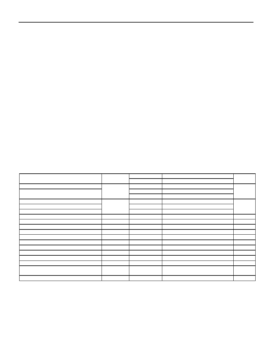
AC ELECTRICAL CHARACTERISTICS (MULTIPLEXED ADDRESS/DATA BUS)
(Note 1)
(VCC3 = 3.0V to 3.6V, VCC1 = 1.8V ±10%, TA = -40°C to +85°C.)
PARAMETER
SYMBOL
75MHz
VARIABLE CLOCK
UNITS
MIN
MAX
MIN
MAX
External Crystal Frequency
1 / tCLK
4
40
MHz
Clock Mutliplier 2X Mode
Clock Multiplier 4X Mode
16
37.5
11
18.75
External Clock Oscillator Frequency
1 / tCLK
DC
75
MHz
Clock Mutliplier 2X Mode
16
37.5
Clock Multiplier 4X Mode
11
18.75
ALE Pulse Width
15.0
tCLCL + tCHCL - 5
ns
Port 0 Instruction Address Valid to ALE Low
tLHLL
1.7
tCHCL - 5
ns
Address Hold After ALE Low
tAVLL
4.7
tCLCH - 2
ns
ALE Low to Valid Instruction In
tLLAX
14.3
2tCLCL + tCLCH - 19
ns
ALE Low to PSEN Low
tLLIV
3.7
tCLCH - 3
ns
PSEN
Pulse Width
tLLPL
21.7
2tCLCL - 5
ns
PSEN
Low to Valid Instruction In
tPLPH
9.7
2tCLCL -17
ns
Input Instruction Hold After PSEN
tPLIV
0
ns
Input Instruction Float After PSEN
tPXIX
8.3
tCLCL - 5
ns
Port 0 Address to Valid Instruction In
tAVIV0
21.0
3tCLCL - 19
ns
Port 2, 4, 6 Address or Port 4 CE to Valid
Instruction In
tAVIV2
27.7
3tCLCL + tCLCH - 19
ns
PSEN
Low to Address Float
tPLAZ
0
ns
Note 1: Specifications to -40°C are guaranteed by design and not production tested.
Note 2: All parameters apply to both commercial and industrial temperature operation, unless otherwise noted.
Note 3: tCLCL, tCLCH, tCHCL are time periods associated with the internal system clock and are related to the external clock (tCLK) as defined in the
External Clock Oscillator (XTAL1) Characteristics table.
Note 4: The precalculated 75MHz MIN/MAX timing specifications assume an exact 50% duty cycle.
Note 5: All signals guaranteed with load capacitance of 80pF except Port 0, Port 2, ALE, PSEN, RD, and WR with 100pF. The following signals,
when configured for memory interface, are also characterized with 100pF loading: Port 4 (CE0-3, A16–A19), Port 5.4–5.7 ( PCE0-3),
Port 6.0–6.5 (CE4-7, A20, A21), Port 7 (demultiplexed mode A0–A7).
Note 6: For high-frequency operation, special attention should be paid to the float times of the interfaced memory devices so as to avoid bus
contention.
Note 7: References to the XTAL, XTAL1 or CLK signal in timing diagrams is to assist in determining the relative occurrence of events, not for
determing absolute signal timing with respect to the external clock.
相关PDF资料 |
PDF描述 |
|---|---|
| VE-B43-IX-F1 | CONVERTER MOD DC/DC 24V 75W |
| DS89C450-ENL+ | IC MCU FLASH 64KB 33MHZ 44-TQFP |
| VE-B43-IW-F3 | CONVERTER MOD DC/DC 24V 100W |
| DS89C450-MNL+ | IC MCU FLASH 64KB 33MHZ 40-DIP |
| VE-B43-IW-F2 | CONVERTER MOD DC/DC 24V 100W |
相关代理商/技术参数 |
参数描述 |
|---|---|
| DS80C400-FNY+ | 功能描述:8位微控制器 -MCU Network MCU RoHS:否 制造商:Silicon Labs 核心:8051 处理器系列:C8051F39x 数据总线宽度:8 bit 最大时钟频率:50 MHz 程序存储器大小:16 KB 数据 RAM 大小:1 KB 片上 ADC:Yes 工作电源电压:1.8 V to 3.6 V 工作温度范围:- 40 C to + 105 C 封装 / 箱体:QFN-20 安装风格:SMD/SMT |
| DS80C400-KIT | 功能描述:EVAL KIT FOR DS80C400 RoHS:否 类别:编程器,开发系统 >> 通用嵌入式开发板和套件(MCU、DSP、FPGA、CPLD等) 系列:- 产品培训模块:Blackfin® Processor Core Architecture Overview Blackfin® Device Drivers Blackfin® Optimizations for Performance and Power Consumption Blackfin® System Services 特色产品:Blackfin? BF50x Series Processors 标准包装:1 系列:Blackfin® 类型:DSP 适用于相关产品:ADSP-BF548 所含物品:板,软件,4x4 键盘,光学拨轮,QVGA 触摸屏 LCD 和 40G 硬盘 配用:ADZS-BFBLUET-EZEXT-ND - EZ-EXTENDER DAUGHTERBOARDADZS-BFLLCD-EZEXT-ND - BOARD EXT LANDSCAP LCD INTERFACE 相关产品:ADSP-BF542BBCZ-4A-ND - IC DSP 16BIT 400MHZ 400CSBGAADSP-BF544MBBCZ-5M-ND - IC DSP 16BIT 533MHZ MDDR 400CBGAADSP-BF542MBBCZ-5M-ND - IC DSP 16BIT 533MHZ MDDR 400CBGAADSP-BF542KBCZ-6A-ND - IC DSP 16BIT 600MHZ 400CSBGAADSP-BF547MBBCZ-5M-ND - IC DSP 16BIT 533MHZ MDDR 400CBGAADSP-BF548BBCZ-5A-ND - IC DSP 16BIT 533MHZ 400CSBGAADSP-BF547BBCZ-5A-ND - IC DSP 16BIT 533MHZ 400CSBGAADSP-BF544BBCZ-5A-ND - IC DSP 16BIT 533MHZ 400CSBGAADSP-BF542BBCZ-5A-ND - IC DSP 16BIT 533MHZ 400CSBGA |
| DS80C400-KIT# | 功能描述:开发板和工具包 - 8051 RoHS:否 制造商:Silicon Labs 产品:Development Kits 工具用于评估:C8051F960, Si7005 核心: 接口类型:USB 工作电源电压: |
| DS80C410 | 制造商:MAXIM 制造商全称:Maxim Integrated Products 功能描述:Network Microcontrollers with Ethernet and CAN |
| DS80C410_09 | 制造商:MAXIM 制造商全称:Maxim Integrated Products 功能描述:Network Microcontrollers with Ethernet and CAN |
发布紧急采购,3分钟左右您将得到回复。