- 您现在的位置:买卖IC网 > PDF目录19362 > DSP56311VF150R2 (Freescale Semiconductor)IC DSP 24BIT 150MHZ 196-BGA PDF资料下载
参数资料
| 型号: | DSP56311VF150R2 |
| 厂商: | Freescale Semiconductor |
| 文件页数: | 10/96页 |
| 文件大小: | 0K |
| 描述: | IC DSP 24BIT 150MHZ 196-BGA |
| 标准包装: | 750 |
| 系列: | DSP56K/Symphony |
| 类型: | 定点 |
| 接口: | 主机接口,SSI,SCI |
| 时钟速率: | 150MHz |
| 非易失内存: | ROM(576 B) |
| 芯片上RAM: | 384kB |
| 电压 - 输入/输出: | 3.30V |
| 电压 - 核心: | 1.80V |
| 工作温度: | -40°C ~ 100°C |
| 安装类型: | 表面贴装 |
| 封装/外壳: | 196-LBGA |
| 供应商设备封装: | 196-MAPBGA(15x15) |
| 包装: | 带卷 (TR) |
第1页第2页第3页第4页第5页第6页第7页第8页第9页当前第10页第11页第12页第13页第14页第15页第16页第17页第18页第19页第20页第21页第22页第23页第24页第25页第26页第27页第28页第29页第30页第31页第32页第33页第34页第35页第36页第37页第38页第39页第40页第41页第42页第43页第44页第45页第46页第47页第48页第49页第50页第51页第52页第53页第54页第55页第56页第57页第58页第59页第60页第61页第62页第63页第64页第65页第66页第67页第68页第69页第70页第71页第72页第73页第74页第75页第76页第77页第78页第79页第80页第81页第82页第83页第84页第85页第86页第87页第88页第89页第90页第91页第92页第93页第94页第95页第96页
DSP56311 Technical Data, Rev. 8
1-14
Freescale Semiconductor
Signals/Connections
1.11 Timers
The DSP56311 has three identical and independent timers. Each timer can use internal or external clocking and can
either interrupt the DSP56311 after a specified number of events (clocks) or signal an external device after
counting a specific number of internal events.
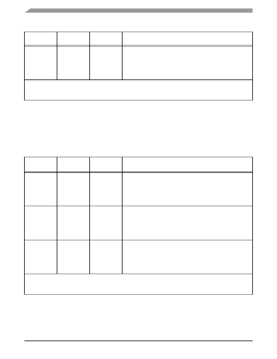
SCLK
PE2
Input/Output
Input or Output
Ignored Input
Serial Clock—Provides the input or output clock used by the transmitter and/or
the receiver.
Port E 2—The default configuration following reset is GPIO input PE2. When
configured as PE2, signal direction is controlled through the Port E Direction
Register. The signal can be configured as an SCI signal SCLK through the Port
E Control Register.
Notes:
1.
In the Stop state, the signal maintains the last state as follows:
If the last state is input, the signal is an ignored input.
If the last state is output, these lines have weak keepers that maintain the last output state even if the drivers are tri-stated.
2.
The Wait processing state does not affect the signal state.
Table 1-15.
Triple Timer Signals
Signal Name
Type
State During
Reset1,2
Signal Description
TIO0
Input or Output
Ignored Input
Timer 0 Schmitt-Trigger Input/Output— When Timer 0 functions as an
external event counter or in measurement mode, TIO0 is used as input. When
Timer 0 functions in watchdog, timer, or pulse modulation mode, TIO0 is used
as output.
The default mode after reset is GPIO input. TIO0 can be changed to output or
configured as a timer I/O through the Timer 0 Control/Status Register (TCSR0).
TIO1
Input or Output
Ignored Input
Timer 1 Schmitt-Trigger Input/Output— When Timer 1 functions as an
external event counter or in measurement mode, TIO1 is used as input. When
Timer 1 functions in watchdog, timer, or pulse modulation mode, TIO1 is used
as output.
The default mode after reset is GPIO input. TIO1 can be changed to output or
configured as a timer I/O through the Timer 1 Control/Status Register (TCSR1).
TIO2
Input or Output
Ignored Input
Timer 2 Schmitt-Trigger Input/Output— When Timer 2 functions as an
external event counter or in measurement mode, TIO2 is used as input. When
Timer 2 functions in watchdog, timer, or pulse modulation mode, TIO2 is used
as output.
The default mode after reset is GPIO input. TIO2 can be changed to output or
configured as a timer I/O through the Timer 2 Control/Status Register (TCSR2).
Notes:
1.
In the Stop state, the signal maintains the last state as follows:
If the last state is input, the signal is an ignored input.
If the last state is output, these lines have weak keepers that maintain the last output state even if the drivers are tri-stated.
2.
The Wait processing state does not affect the signal state.
Table 1-14.
Serial Communication Interface (Continued)
Signal Name
Type
State During
Reset1,2
Signal Description
相关PDF资料 |
PDF描述 |
|---|---|
| UBA2016AP/1,112 | IC LAMP DVR FLUORES 600V 20-DIP |
| T525D477M2R5ATE025 | CAP TANT 470UF 2.5V 20% 2917 |
| RBM12DCWS | CONN EDGECARD 24POS DIP .156 SLD |
| AGL125V2-FGG144 | IC FPGA IGLOO 1.2-1.5V 144FPBGA |
| T525D337M003ATE025 | CAP TANT 330UF 3V 20% 2917 |
相关代理商/技术参数 |
参数描述 |
|---|---|
| DSP56311VF160 | 功能描述:数字信号处理器和控制器 - DSP, DSC SSP26111VF160A RoHS:否 制造商:Microchip Technology 核心:dsPIC 数据总线宽度:16 bit 程序存储器大小:16 KB 数据 RAM 大小:2 KB 最大时钟频率:40 MHz 可编程输入/输出端数量:35 定时器数量:3 设备每秒兆指令数:50 MIPs 工作电源电压:3.3 V 最大工作温度:+ 85 C 封装 / 箱体:TQFP-44 安装风格:SMD/SMT |
| DSP56311VL150 | 功能描述:数字信号处理器和控制器 - DSP, DSC 24 BIT DSP PBFREE RoHS:否 制造商:Microchip Technology 核心:dsPIC 数据总线宽度:16 bit 程序存储器大小:16 KB 数据 RAM 大小:2 KB 最大时钟频率:40 MHz 可编程输入/输出端数量:35 定时器数量:3 设备每秒兆指令数:50 MIPs 工作电源电压:3.3 V 最大工作温度:+ 85 C 封装 / 箱体:TQFP-44 安装风格:SMD/SMT |
| DSP56311VL150B1 | 功能描述:数字信号处理器和控制器 - DSP, DSC 24 BIT DSP PBFREE RoHS:否 制造商:Microchip Technology 核心:dsPIC 数据总线宽度:16 bit 程序存储器大小:16 KB 数据 RAM 大小:2 KB 最大时钟频率:40 MHz 可编程输入/输出端数量:35 定时器数量:3 设备每秒兆指令数:50 MIPs 工作电源电压:3.3 V 最大工作温度:+ 85 C 封装 / 箱体:TQFP-44 安装风格:SMD/SMT |
| DSP56311VL150R2 | 功能描述:数字信号处理器和控制器 - DSP, DSC 24 BIT DSP PBFREE RoHS:否 制造商:Microchip Technology 核心:dsPIC 数据总线宽度:16 bit 程序存储器大小:16 KB 数据 RAM 大小:2 KB 最大时钟频率:40 MHz 可编程输入/输出端数量:35 定时器数量:3 设备每秒兆指令数:50 MIPs 工作电源电压:3.3 V 最大工作温度:+ 85 C 封装 / 箱体:TQFP-44 安装风格:SMD/SMT |
| DSP56311VL160 | 功能描述:数字信号处理器和控制器 - DSP, DSC 24 BIT DSP PBFREE RoHS:否 制造商:Microchip Technology 核心:dsPIC 数据总线宽度:16 bit 程序存储器大小:16 KB 数据 RAM 大小:2 KB 最大时钟频率:40 MHz 可编程输入/输出端数量:35 定时器数量:3 设备每秒兆指令数:50 MIPs 工作电源电压:3.3 V 最大工作温度:+ 85 C 封装 / 箱体:TQFP-44 安装风格:SMD/SMT |
发布紧急采购,3分钟左右您将得到回复。