- 您现在的位置:买卖IC网 > PDF目录19362 > DSP56311VF150R2 (Freescale Semiconductor)IC DSP 24BIT 150MHZ 196-BGA PDF资料下载
参数资料
| 型号: | DSP56311VF150R2 |
| 厂商: | Freescale Semiconductor |
| 文件页数: | 21/96页 |
| 文件大小: | 0K |
| 描述: | IC DSP 24BIT 150MHZ 196-BGA |
| 标准包装: | 750 |
| 系列: | DSP56K/Symphony |
| 类型: | 定点 |
| 接口: | 主机接口,SSI,SCI |
| 时钟速率: | 150MHz |
| 非易失内存: | ROM(576 B) |
| 芯片上RAM: | 384kB |
| 电压 - 输入/输出: | 3.30V |
| 电压 - 核心: | 1.80V |
| 工作温度: | -40°C ~ 100°C |
| 安装类型: | 表面贴装 |
| 封装/外壳: | 196-LBGA |
| 供应商设备封装: | 196-MAPBGA(15x15) |
| 包装: | 带卷 (TR) |
第1页第2页第3页第4页第5页第6页第7页第8页第9页第10页第11页第12页第13页第14页第15页第16页第17页第18页第19页第20页当前第21页第22页第23页第24页第25页第26页第27页第28页第29页第30页第31页第32页第33页第34页第35页第36页第37页第38页第39页第40页第41页第42页第43页第44页第45页第46页第47页第48页第49页第50页第51页第52页第53页第54页第55页第56页第57页第58页第59页第60页第61页第62页第63页第64页第65页第66页第67页第68页第69页第70页第71页第72页第73页第74页第75页第76页第77页第78页第79页第80页第81页第82页第83页第84页第85页第86页第87页第88页第89页第90页第91页第92页第93页第94页第95页第96页
DSP56311 Technical Data, Rev. 8
2-8
Freescale Semiconductor
Specifications
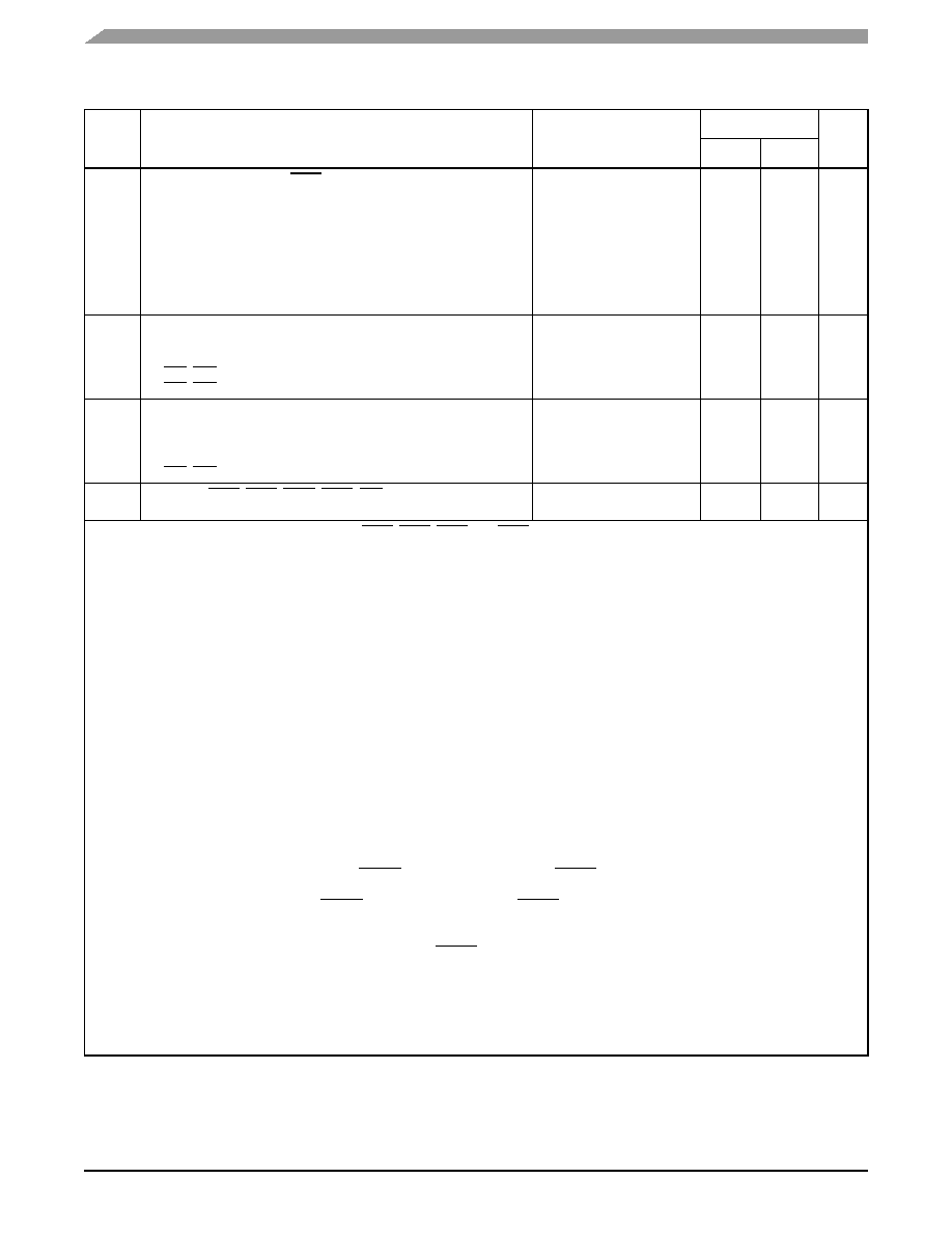
26
Duration of level sensitive IRQA assertion to ensure interrupt service
(when exiting Stop)
2, 3
PLL is not active during Stop (PCTL Bit 17 = 0) and Stop delay is
enabled
(Operating Mode Register Bit 6 = 0)
PLL is not active during Stop (PCTL Bit 17 = 0) and Stop delay is
not enabled
(Operating Mode Register Bit 6 = 1)
PLL is active during Stop (PCTL Bit 17 = 1) (implies no Stop delay)
Minimum:
PLC
× ET
C × PDF + (128K
PLC/2)
× TC
PLC
× ET
C × PDF +
(20.5
± 0.5) × TC
5.5
× T
C
13.6
12.3
36.7
—
ms
ns
27
Interrupt Request Rate
HI08, ESSI, SCI, Timer
DMA
IRQ, NMI (edge trigger)
IRQ, NMI (level trigger)
Maximum:
12
× T
C
8
× TC
8
× TC
12
× T
C
—
80.0
53.3
80.0
ns
28
DMA Request Rate
Data read from HI08, ESSI, SCI
Data write to HI08, ESSI, SCI
Timer
IRQ, NMI (edge trigger)
Maximum:
6
× T
C
7
× TC
2
× TC
3
× T
C
—
40.0
46.7
13.3
20.0
ns
29
Delay from IRQA, IRQB, IRQC, IRQD, NMI assertion to external
memory (DMA source) access address out valid
Minimum:
4.25
× T
C + 2.0
30.3
—
ns
Notes:
1.
When fast interrupts are used and IRQA, IRQB, IRQC, and IRQD are defined as level-sensitive, timings 19 through 21 apply to
prevent multiple interrupt service. To avoid these timing restrictions, the deasserted Edge-triggered mode is recommended
when fast interrupts are used. Long interrupts are recommended for Level-sensitive mode.
2.
This timing depends on several settings:
For PLL disable, using internal oscillator (PLL Control Register (PCTL) Bit 16 = 0) and oscillator disabled during Stop (PCTL
Bit 17 = 0), a stabilization delay is required to assure that the oscillator is stable before programs are executed. Resetting the
Stop delay (Operating Mode Register Bit 6 = 0) provides the proper delay. While Operating Mode Register Bit 6 = 1 can be set,
it is not recommended, and these specifications do not guarantee timings for that case.
For PLL disable, using internal oscillator (PCTL Bit 16 = 0) and oscillator enabled during Stop (PCTL Bit 17=1), no
stabilization delay is required and recovery is minimal (Operating Mode Register Bit 6 setting is ignored).
For PLL disable, using external clock (PCTL Bit 16 = 1), no stabilization delay is required and recovery time is defined by the
PCTL Bit 17 and Operating Mode Register Bit 6 settings.
For PLL enable, if PCTL Bit 17 is 0, the PLL is shutdown during Stop. Recovering from Stop requires the PLL to get locked.
The PLL lock procedure duration, PLL Lock Cycles (PLC), may be in the range of 0 to 1000 cycles. This procedure occurs in
parallel with the stop delay counter, and stop recovery ends when the last of these two events occurs. The stop delay counter
completes count or PLL lock procedure completion.
PLC value for PLL disable is 0.
The maximum value for ETC is 4096 (maximum MF) divided by the desired internal frequency (that is, for 66 MHz it is 4096/66
MHz = 62
s). During the stabilization period, TC, TH, and TL is not constant, and their width may vary, so timing may vary as
well.
3.
Periodically sampled and not 100 percent tested.
4.
Value depends on clock source:
For an external clock generator, RESET duration is measured while RESET is asserted, VCC is valid, and the EXTAL input is
active and valid.
For an internal oscillator, RESET duration is measured while RESET is asserted and VCC is valid. The specified timing
reflects the crystal oscillator stabilization time after power-up. This number is affected both by the specifications of the crystal
and other components connected to the oscillator and reflects worst case conditions.
When the VCC is valid, but the other “required RESET duration” conditions (as specified above) have not been yet met, the
device circuitry is in an uninitialized state that can result in significant power consumption and heat-up. Designs should
minimize this state to the shortest possible duration.
5.
If PLL does not lose lock.
6.
VCCQH = 3.3 V ± 0.3 V, VCC = 1.8 V ± 0.1 V; TJ = –40°C to +100°C, CL = 50 pF.
7.
WS = number of wait states (measured in clock cycles, number of TC).
8.
Use expression to compute maximum value.
Table 2-7.
Reset, Stop, Mode Select, and Interrupt Timing6 (Continued)
No.
Characteristics
Expression
150 MHz
Unit
Min
Max
相关PDF资料 |
PDF描述 |
|---|---|
| UBA2016AP/1,112 | IC LAMP DVR FLUORES 600V 20-DIP |
| T525D477M2R5ATE025 | CAP TANT 470UF 2.5V 20% 2917 |
| RBM12DCWS | CONN EDGECARD 24POS DIP .156 SLD |
| AGL125V2-FGG144 | IC FPGA IGLOO 1.2-1.5V 144FPBGA |
| T525D337M003ATE025 | CAP TANT 330UF 3V 20% 2917 |
相关代理商/技术参数 |
参数描述 |
|---|---|
| DSP56311VF160 | 功能描述:数字信号处理器和控制器 - DSP, DSC SSP26111VF160A RoHS:否 制造商:Microchip Technology 核心:dsPIC 数据总线宽度:16 bit 程序存储器大小:16 KB 数据 RAM 大小:2 KB 最大时钟频率:40 MHz 可编程输入/输出端数量:35 定时器数量:3 设备每秒兆指令数:50 MIPs 工作电源电压:3.3 V 最大工作温度:+ 85 C 封装 / 箱体:TQFP-44 安装风格:SMD/SMT |
| DSP56311VL150 | 功能描述:数字信号处理器和控制器 - DSP, DSC 24 BIT DSP PBFREE RoHS:否 制造商:Microchip Technology 核心:dsPIC 数据总线宽度:16 bit 程序存储器大小:16 KB 数据 RAM 大小:2 KB 最大时钟频率:40 MHz 可编程输入/输出端数量:35 定时器数量:3 设备每秒兆指令数:50 MIPs 工作电源电压:3.3 V 最大工作温度:+ 85 C 封装 / 箱体:TQFP-44 安装风格:SMD/SMT |
| DSP56311VL150B1 | 功能描述:数字信号处理器和控制器 - DSP, DSC 24 BIT DSP PBFREE RoHS:否 制造商:Microchip Technology 核心:dsPIC 数据总线宽度:16 bit 程序存储器大小:16 KB 数据 RAM 大小:2 KB 最大时钟频率:40 MHz 可编程输入/输出端数量:35 定时器数量:3 设备每秒兆指令数:50 MIPs 工作电源电压:3.3 V 最大工作温度:+ 85 C 封装 / 箱体:TQFP-44 安装风格:SMD/SMT |
| DSP56311VL150R2 | 功能描述:数字信号处理器和控制器 - DSP, DSC 24 BIT DSP PBFREE RoHS:否 制造商:Microchip Technology 核心:dsPIC 数据总线宽度:16 bit 程序存储器大小:16 KB 数据 RAM 大小:2 KB 最大时钟频率:40 MHz 可编程输入/输出端数量:35 定时器数量:3 设备每秒兆指令数:50 MIPs 工作电源电压:3.3 V 最大工作温度:+ 85 C 封装 / 箱体:TQFP-44 安装风格:SMD/SMT |
| DSP56311VL160 | 功能描述:数字信号处理器和控制器 - DSP, DSC 24 BIT DSP PBFREE RoHS:否 制造商:Microchip Technology 核心:dsPIC 数据总线宽度:16 bit 程序存储器大小:16 KB 数据 RAM 大小:2 KB 最大时钟频率:40 MHz 可编程输入/输出端数量:35 定时器数量:3 设备每秒兆指令数:50 MIPs 工作电源电压:3.3 V 最大工作温度:+ 85 C 封装 / 箱体:TQFP-44 安装风格:SMD/SMT |
发布紧急采购,3分钟左右您将得到回复。