- 您现在的位置:买卖IC网 > PDF目录19362 > DSP56311VF150R2 (Freescale Semiconductor)IC DSP 24BIT 150MHZ 196-BGA PDF资料下载
参数资料
| 型号: | DSP56311VF150R2 |
| 厂商: | Freescale Semiconductor |
| 文件页数: | 53/96页 |
| 文件大小: | 0K |
| 描述: | IC DSP 24BIT 150MHZ 196-BGA |
| 标准包装: | 750 |
| 系列: | DSP56K/Symphony |
| 类型: | 定点 |
| 接口: | 主机接口,SSI,SCI |
| 时钟速率: | 150MHz |
| 非易失内存: | ROM(576 B) |
| 芯片上RAM: | 384kB |
| 电压 - 输入/输出: | 3.30V |
| 电压 - 核心: | 1.80V |
| 工作温度: | -40°C ~ 100°C |
| 安装类型: | 表面贴装 |
| 封装/外壳: | 196-LBGA |
| 供应商设备封装: | 196-MAPBGA(15x15) |
| 包装: | 带卷 (TR) |
第1页第2页第3页第4页第5页第6页第7页第8页第9页第10页第11页第12页第13页第14页第15页第16页第17页第18页第19页第20页第21页第22页第23页第24页第25页第26页第27页第28页第29页第30页第31页第32页第33页第34页第35页第36页第37页第38页第39页第40页第41页第42页第43页第44页第45页第46页第47页第48页第49页第50页第51页第52页当前第53页第54页第55页第56页第57页第58页第59页第60页第61页第62页第63页第64页第65页第66页第67页第68页第69页第70页第71页第72页第73页第74页第75页第76页第77页第78页第79页第80页第81页第82页第83页第84页第85页第86页第87页第88页第89页第90页第91页第92页第93页第94页第95页第96页
AC Electrical Characteristics
DSP56311 Technical Data, Rev. 8
Freescale Semiconductor
2-37
2.4.10.2 With an Operating Frequency above 100 MHz
The following considerations can be helpful when GPIO is used for output or input with an operating frequency
above 100 MHz (that is, when CLKOUT is not available).
GPIO as Output:
— The time from fetch of the instruction that changes the GPIO pin to the actual change is seven core
clock cycles. This is true, assuming that the instruction is a one-cycle instruction and that there are no
pipeline stalls or any other pipeline delays.
— The maximum rise or fall time of a GPIO pin is 13 ns (TTL levels, assuming that the maximum of 50
pF load limit is met).
GPIO as Input—GPIO inputs are not synchronized with the core clock. When only one GPIO bit is polled,
this lack of synchronization presents no problem, since the read value can be either the previous value or
the new value of the corresponding GPIO pin. However, there is the risk of reading an intermediate state if:
— Two or more GPIO bits are treated as a coupled group (for example, four possible status states encoded
in two bits).
— The read operation occurs during a simultaneous change of GPIO pins (for example, the change of 00
to 11 may happen through an intermediate state of 01 or 10).
Therefore, when GPIO bits are read, the recommended practice is to poll continuously until two
consecutive read operations have identical results.
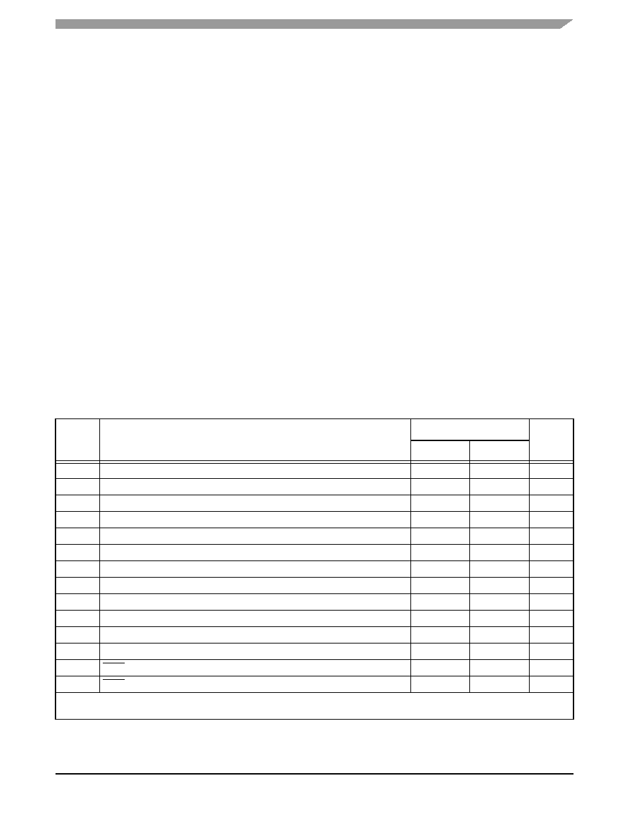
2.4.11 JTAG Timing
Table 2-19.
JTAG Timing
No.
Characteristics
All frequencies
Unit
Min
Max
500
TCK frequency of operation (1/(T
C ×
3); maximum 22 MHz)
0.0
22.0
MHz
501
TCK cycle time in Crystal mode
45.0
—
ns
502
TCK clock pulse width measured at 1.5 V
20.0
—
ns
503
TCK rise and fall times
0.0
3.0
ns
504
Boundary scan input data set-up time
5.0
—
ns
505
Boundary scan input data hold time
24.0
—
ns
506
TCK low to output data valid
0.0
40.0
ns
507
TCK low to output high impedance
0.0
40.0
ns
508
TMS, TDI data set-up time
5.0
—
ns
509
TMS, TDI data hold time
25.0
—
ns
510
TCK low to TDO data valid
0.0
44.0
ns
511
TCK low to TDO high impedance
0.0
44.0
ns
512
TRST assert time
100.0
—
ns
513
TRST set-up time to TCK low
40.0
—
ns
Notes:
1.
VCCQH = 3.3 V ± 0.3 V, VCC = 1.8 V ± 0.1 V; TJ = –40°C to +100 °C, CL = 50 pF.
2.
All timings apply to OnCE module data transfers because it uses the JTAG port as an interface.
相关PDF资料 |
PDF描述 |
|---|---|
| UBA2016AP/1,112 | IC LAMP DVR FLUORES 600V 20-DIP |
| T525D477M2R5ATE025 | CAP TANT 470UF 2.5V 20% 2917 |
| RBM12DCWS | CONN EDGECARD 24POS DIP .156 SLD |
| AGL125V2-FGG144 | IC FPGA IGLOO 1.2-1.5V 144FPBGA |
| T525D337M003ATE025 | CAP TANT 330UF 3V 20% 2917 |
相关代理商/技术参数 |
参数描述 |
|---|---|
| DSP56311VF160 | 功能描述:数字信号处理器和控制器 - DSP, DSC SSP26111VF160A RoHS:否 制造商:Microchip Technology 核心:dsPIC 数据总线宽度:16 bit 程序存储器大小:16 KB 数据 RAM 大小:2 KB 最大时钟频率:40 MHz 可编程输入/输出端数量:35 定时器数量:3 设备每秒兆指令数:50 MIPs 工作电源电压:3.3 V 最大工作温度:+ 85 C 封装 / 箱体:TQFP-44 安装风格:SMD/SMT |
| DSP56311VL150 | 功能描述:数字信号处理器和控制器 - DSP, DSC 24 BIT DSP PBFREE RoHS:否 制造商:Microchip Technology 核心:dsPIC 数据总线宽度:16 bit 程序存储器大小:16 KB 数据 RAM 大小:2 KB 最大时钟频率:40 MHz 可编程输入/输出端数量:35 定时器数量:3 设备每秒兆指令数:50 MIPs 工作电源电压:3.3 V 最大工作温度:+ 85 C 封装 / 箱体:TQFP-44 安装风格:SMD/SMT |
| DSP56311VL150B1 | 功能描述:数字信号处理器和控制器 - DSP, DSC 24 BIT DSP PBFREE RoHS:否 制造商:Microchip Technology 核心:dsPIC 数据总线宽度:16 bit 程序存储器大小:16 KB 数据 RAM 大小:2 KB 最大时钟频率:40 MHz 可编程输入/输出端数量:35 定时器数量:3 设备每秒兆指令数:50 MIPs 工作电源电压:3.3 V 最大工作温度:+ 85 C 封装 / 箱体:TQFP-44 安装风格:SMD/SMT |
| DSP56311VL150R2 | 功能描述:数字信号处理器和控制器 - DSP, DSC 24 BIT DSP PBFREE RoHS:否 制造商:Microchip Technology 核心:dsPIC 数据总线宽度:16 bit 程序存储器大小:16 KB 数据 RAM 大小:2 KB 最大时钟频率:40 MHz 可编程输入/输出端数量:35 定时器数量:3 设备每秒兆指令数:50 MIPs 工作电源电压:3.3 V 最大工作温度:+ 85 C 封装 / 箱体:TQFP-44 安装风格:SMD/SMT |
| DSP56311VL160 | 功能描述:数字信号处理器和控制器 - DSP, DSC 24 BIT DSP PBFREE RoHS:否 制造商:Microchip Technology 核心:dsPIC 数据总线宽度:16 bit 程序存储器大小:16 KB 数据 RAM 大小:2 KB 最大时钟频率:40 MHz 可编程输入/输出端数量:35 定时器数量:3 设备每秒兆指令数:50 MIPs 工作电源电压:3.3 V 最大工作温度:+ 85 C 封装 / 箱体:TQFP-44 安装风格:SMD/SMT |
发布紧急采购,3分钟左右您将得到回复。