- 您现在的位置:买卖IC网 > PDF目录19362 > DSP56311VF150R2 (Freescale Semiconductor)IC DSP 24BIT 150MHZ 196-BGA PDF资料下载
参数资料
| 型号: | DSP56311VF150R2 |
| 厂商: | Freescale Semiconductor |
| 文件页数: | 17/96页 |
| 文件大小: | 0K |
| 描述: | IC DSP 24BIT 150MHZ 196-BGA |
| 标准包装: | 750 |
| 系列: | DSP56K/Symphony |
| 类型: | 定点 |
| 接口: | 主机接口,SSI,SCI |
| 时钟速率: | 150MHz |
| 非易失内存: | ROM(576 B) |
| 芯片上RAM: | 384kB |
| 电压 - 输入/输出: | 3.30V |
| 电压 - 核心: | 1.80V |
| 工作温度: | -40°C ~ 100°C |
| 安装类型: | 表面贴装 |
| 封装/外壳: | 196-LBGA |
| 供应商设备封装: | 196-MAPBGA(15x15) |
| 包装: | 带卷 (TR) |
第1页第2页第3页第4页第5页第6页第7页第8页第9页第10页第11页第12页第13页第14页第15页第16页当前第17页第18页第19页第20页第21页第22页第23页第24页第25页第26页第27页第28页第29页第30页第31页第32页第33页第34页第35页第36页第37页第38页第39页第40页第41页第42页第43页第44页第45页第46页第47页第48页第49页第50页第51页第52页第53页第54页第55页第56页第57页第58页第59页第60页第61页第62页第63页第64页第65页第66页第67页第68页第69页第70页第71页第72页第73页第74页第75页第76页第77页第78页第79页第80页第81页第82页第83页第84页第85页第86页第87页第88页第89页第90页第91页第92页第93页第94页第95页第96页
DSP56311 Technical Data, Rev. 8
2-4
Freescale Semiconductor
Specifications
2.4 AC Electrical Characteristics
The timing waveforms shown in the AC electrical characteristics section are tested with a VIL maximum of 0.3 V
and a VIH minimum of 2.4 V for all pins except EXTAL, which is tested using the input levels shown in Note 6 of
Table 2-2. AC timing specifications, which are referenced to a device input signal, are measured in production with
respect to the 50 percent point of the respective input signal’s transition. DSP56311 output levels are measured
with the production test machine VOL and VOH reference levels set at 0.4 V and 2.4 V, respectively.
Note:
Although the minimum value for the frequency of EXTAL is 0 MHz, the device AC test conditions are 15
MHz and rated speed.
2.4.1
Internal Clocks
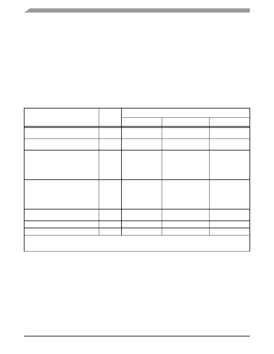
Table 2-4.
Internal Clocks
Characteristics
Symbol
Expression
Min
Typ
Max
Internal operation frequency with PLL
enabled
f—
(Ef
× MF)/
(PDF
× DF)
—
Internal operation frequency with PLL
disabled
f—
Ef/2
—
Internal clock high period
With PLL disabled
With PLL enabled and MF
≤4
With PLL enabled and MF > 4
TH
—
0.49
× ET
C ×
PDF
× DF/MF
0.47
× ETC ×
PDF
× DF/MF
ETC
—
0.51
× ET
C ×
PDF
× DF/MF
0.53
× ETC ×
PDF
× DF/MF
Internal clock low period
With PLL disabled
With PLL enabled and
MF
≤4
With PLL enabled and
MF > 4
TL
—
0.49
× ET
C ×
PDF
× DF/MF
0.47
× ETC ×
PDF
× DF/MF
ETC
—
0.51
× ET
C ×
PDF
× DF/MF
0.53
× ETC ×
PDF
× DF/MF
Internal clock cycle time with PLL enabled
TC
—ETC × PDF ×
DF/MF
—
Internal clock cycle time with PLL disabled
TC
—2
× ET
C
—
Instruction cycle time
ICYC
—TC
—
Notes:
1.
DF = Division Factor; Ef = External frequency; ETC = External clock cycle; MF = Multiplication Factor;
PDF = Predivision Factor; TC = internal clock cycle.
2.
See the PLL and Clock Generation section in the
DSP56300 Family Manual for a details on the PLL.
相关PDF资料 |
PDF描述 |
|---|---|
| UBA2016AP/1,112 | IC LAMP DVR FLUORES 600V 20-DIP |
| T525D477M2R5ATE025 | CAP TANT 470UF 2.5V 20% 2917 |
| RBM12DCWS | CONN EDGECARD 24POS DIP .156 SLD |
| AGL125V2-FGG144 | IC FPGA IGLOO 1.2-1.5V 144FPBGA |
| T525D337M003ATE025 | CAP TANT 330UF 3V 20% 2917 |
相关代理商/技术参数 |
参数描述 |
|---|---|
| DSP56311VF160 | 功能描述:数字信号处理器和控制器 - DSP, DSC SSP26111VF160A RoHS:否 制造商:Microchip Technology 核心:dsPIC 数据总线宽度:16 bit 程序存储器大小:16 KB 数据 RAM 大小:2 KB 最大时钟频率:40 MHz 可编程输入/输出端数量:35 定时器数量:3 设备每秒兆指令数:50 MIPs 工作电源电压:3.3 V 最大工作温度:+ 85 C 封装 / 箱体:TQFP-44 安装风格:SMD/SMT |
| DSP56311VL150 | 功能描述:数字信号处理器和控制器 - DSP, DSC 24 BIT DSP PBFREE RoHS:否 制造商:Microchip Technology 核心:dsPIC 数据总线宽度:16 bit 程序存储器大小:16 KB 数据 RAM 大小:2 KB 最大时钟频率:40 MHz 可编程输入/输出端数量:35 定时器数量:3 设备每秒兆指令数:50 MIPs 工作电源电压:3.3 V 最大工作温度:+ 85 C 封装 / 箱体:TQFP-44 安装风格:SMD/SMT |
| DSP56311VL150B1 | 功能描述:数字信号处理器和控制器 - DSP, DSC 24 BIT DSP PBFREE RoHS:否 制造商:Microchip Technology 核心:dsPIC 数据总线宽度:16 bit 程序存储器大小:16 KB 数据 RAM 大小:2 KB 最大时钟频率:40 MHz 可编程输入/输出端数量:35 定时器数量:3 设备每秒兆指令数:50 MIPs 工作电源电压:3.3 V 最大工作温度:+ 85 C 封装 / 箱体:TQFP-44 安装风格:SMD/SMT |
| DSP56311VL150R2 | 功能描述:数字信号处理器和控制器 - DSP, DSC 24 BIT DSP PBFREE RoHS:否 制造商:Microchip Technology 核心:dsPIC 数据总线宽度:16 bit 程序存储器大小:16 KB 数据 RAM 大小:2 KB 最大时钟频率:40 MHz 可编程输入/输出端数量:35 定时器数量:3 设备每秒兆指令数:50 MIPs 工作电源电压:3.3 V 最大工作温度:+ 85 C 封装 / 箱体:TQFP-44 安装风格:SMD/SMT |
| DSP56311VL160 | 功能描述:数字信号处理器和控制器 - DSP, DSC 24 BIT DSP PBFREE RoHS:否 制造商:Microchip Technology 核心:dsPIC 数据总线宽度:16 bit 程序存储器大小:16 KB 数据 RAM 大小:2 KB 最大时钟频率:40 MHz 可编程输入/输出端数量:35 定时器数量:3 设备每秒兆指令数:50 MIPs 工作电源电压:3.3 V 最大工作温度:+ 85 C 封装 / 箱体:TQFP-44 安装风格:SMD/SMT |
发布紧急采购,3分钟左右您将得到回复。