- 您现在的位置:买卖IC网 > PDF目录295865 > E28F200BX-B60 (INTEL CORP) 2-MBIT (128K x 16, 256K x 8) BOOT BLOCK FLASH MEMORY FAMILY PDF资料下载
参数资料
| 型号: | E28F200BX-B60 |
| 厂商: | INTEL CORP |
| 元件分类: | PROM |
| 英文描述: | 2-MBIT (128K x 16, 256K x 8) BOOT BLOCK FLASH MEMORY FAMILY |
| 中文描述: | 128K X 16 FLASH 12V PROM, 60 ns, PDSO56 |
| 封装: | 20 X 14 MM, TSOP-56 |
| 文件页数: | 9/48页 |
| 文件大小: | 453K |
| 代理商: | E28F200BX-B60 |
第1页第2页第3页第4页第5页第6页第7页第8页当前第9页第10页第11页第12页第13页第14页第15页第16页第17页第18页第19页第20页第21页第22页第23页第24页第25页第26页第27页第28页第29页第30页第31页第32页第33页第34页第35页第36页第37页第38页第39页第40页第41页第42页第43页第44页第45页第46页第47页第48页
28F200BX-TB 28F002BX-TB
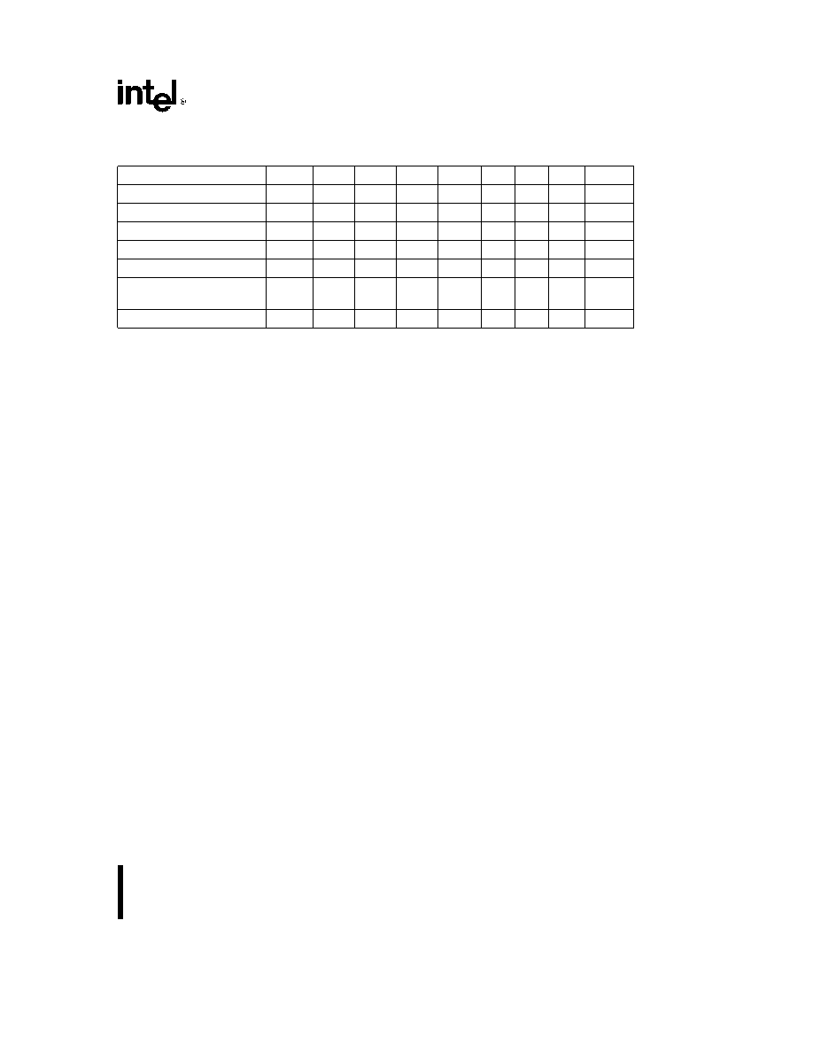
42 28F002BX Bus Operations
Table 3 Bus Operations
Mode
Notes
RP
CE
OE
WE
A9
A0
VPP
DQ0–7
Read
1 2
VIH
VIL
VIH
XX
X
DOUT
Output Disable
VIH
VIL
VIH
X
High Z
Standby
VIH
X
High Z
Deep Power-Down
9
VIL
X
High Z
Intelligent Identifier (Mfr)
3 4
VIH
VIL
VIH
VID
VIL
X
89H
Intelligent Identifier (Device)
3 4 5
VIH
VIL
VIH
VID
VIH
X
7CH
7DH
Write
6 7 8
VIH
VIL
VIH
VIL
XX
X
DIN
NOTES
1 Refer to DC Characteristics
2 X can be VIL or VIH for control pins and addresses VPPL or VPPH for VPP
3 See DC characteristics for VPPL VPPH VHH VID voltages
4 Manufacturer and Device codes may also be accessed via a CUI write sequence A1–A16 e X
5 Device ID e 7CH for 28F002BX-T and 7DH for 28F002BX-B
6 Refer to Table 4 for valid DIN during a write operation
7 Command writes for Block Erase or byte program are only executed when VPP e VPPH
8 Program or erase the Boot block by holding RP
at VHH
9 RP
must be at GND g02V to meet the 12 mA maximum deep power-down current
43 Read Operations
The 2-Mbit boot block flash family has three user
read modes Array Intelligent Identifier and Status
Register Status Register read mode will be dis-
cussed in detail in the ‘‘Write Operations’’ section
During power-up conditions (VCC supply ramping) it
takes a maximum of 600 ns from when VCC is at
45V minimum to valid data on the outputs
431 READ ARRAY
If the memory is not in the Read Array mode it is
necessary to write the appropriate read mode com-
mand to the CUI The 2-Mbit boot block flash family
has three control functions all of which must be
logically active
to obtain data at the outputs
Chip-Enable CE
is the device selection control
Power-Down RP
is the device power control Out-
put-Enable OE
is the DATA INPUTOUTPUT
(DQ 015 or DQ 07 ) direction control and when
active is used to drive data from the selected memo-
ry on to the IO bus
4311 Output Control
With OE
at logic-high level (VIH) the output from
the device is disabled and data inputoutput pins
(DQ 015 or DQ 07 ) are tri-stated Data input is
then controlled by WE
4312 Input Control
With WE
at logic-high level (VIH) input to the de-
vice is disabled Data InputOutput pins (DQ- 015
or DQ 07 ) are controlled by OE
432 INTELLIGENT IDENTlFlERS
28F200BX Products
The manufacturer and device codes are read via the
CUI or by taking the A9 pin to 12V Writing 90H to
the CUI places the device into Intelligent Identifier
read mode A read of location 00000
H outputs the
manufacturer’s identification code 0089H and loca-
tion 00001
H outputs the device code 2274H for
28F200BX-T
2275H
for
28F200BX-B
When
BYTE
is at a logic low only the lower byte of the
above signatures is read and DQ15 Ab1 is a ‘‘don’t
care’’ during Intelligent Identifier mode A read array
command must be written to the CUI to return to the
read array mode
17
相关PDF资料 |
PDF描述 |
|---|---|
| E28F200BX-B80 | 2-MBIT (128K x 16, 256K x 8) BOOT BLOCK FLASH MEMORY FAMILY |
| E28F200BX-T120 | 2-MBIT (128K x 16, 256K x 8) BOOT BLOCK FLASH MEMORY FAMILY |
| E28F002BX-T120 | 2-MBIT (128K x 16, 256K x 8) BOOT BLOCK FLASH MEMORY FAMILY |
| E28F200CV-B60 | 2-MBIT SmartVoltage BOOT BLOCK FLASH MEMORY FAMILY |
| E28F320J5-120 | StrataFlash MEMORY TECHNOLOGY 32 AND 64 MBIT |
相关代理商/技术参数 |
参数描述 |
|---|---|
| E28F200BX-B80 | 制造商:INTEL 制造商全称:Intel Corporation 功能描述:2-MBIT (128K x 16, 256K x 8) BOOT BLOCK FLASH MEMORY FAMILY |
| E28F200BX-L150 | 制造商:未知厂家 制造商全称:未知厂家 功能描述:x8/x16 Flash EEPROM |
| E28F200BX-T120 | 制造商:INTEL 制造商全称:Intel Corporation 功能描述:2-MBIT (128K x 16, 256K x 8) BOOT BLOCK FLASH MEMORY FAMILY |
| E28F200BX-T60 | 制造商:INTEL 制造商全称:Intel Corporation 功能描述:2-MBIT (128K x 16, 256K x 8) BOOT BLOCK FLASH MEMORY FAMILY |
| E28F200BX-T80 | 制造商:INTEL 制造商全称:Intel Corporation 功能描述:2-MBIT (128K x 16, 256K x 8) BOOT BLOCK FLASH MEMORY FAMILY |
发布紧急采购,3分钟左右您将得到回复。