- 您现在的位置:买卖IC网 > PDF目录299030 > EP20K100BC196-2 (ALTERA CORP) LOADABLE PLD, PBGA196 PDF资料下载
参数资料
| 型号: | EP20K100BC196-2 |
| 厂商: | ALTERA CORP |
| 元件分类: | PLD |
| 英文描述: | LOADABLE PLD, PBGA196 |
| 文件页数: | 14/68页 |
| 文件大小: | 975K |
| 代理商: | EP20K100BC196-2 |
第1页第2页第3页第4页第5页第6页第7页第8页第9页第10页第11页第12页第13页当前第14页第15页第16页第17页第18页第19页第20页第21页第22页第23页第24页第25页第26页第27页第28页第29页第30页第31页第32页第33页第34页第35页第36页第37页第38页第39页第40页第41页第42页第43页第44页第45页第46页第47页第48页第49页第50页第51页第52页第53页第54页第55页第56页第57页第58页第59页第60页第61页第62页第63页第64页第65页第66页第67页第68页
21
4317K–AVR–03/2013
AT90PWM2/3/2B/3B
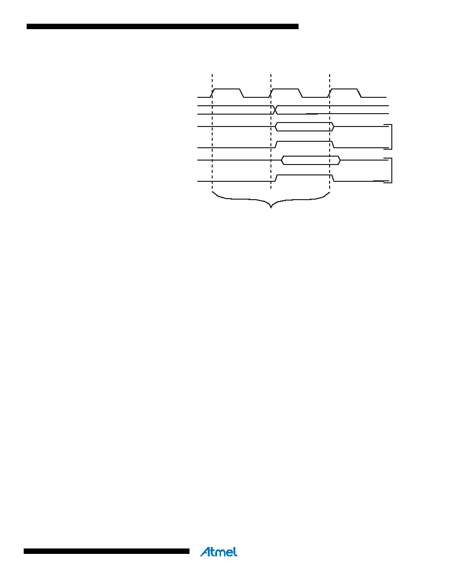
Figure 6-3.
On-chip Data SRAM Access Cycles
6.3
EEPROM Data Memory
The AT90PWM2/2B/3/3B contains 512 bytes of data EEPROM memory. It is organized as a
separate data space, in which single bytes can be read and written. The EEPROM has an
endurance of at least 100,000 write/erase cycles. The access between the EEPROM and the
CPU is described in the following, specifying the EEPROM Address Registers, the EEPROM
Data Register, and the EEPROM Control Register.
For a detailed description of SPI and Parallel data downloading to the EEPROM, see “Serial
mands” on page 284 respectively.
6.3.1
EEPROM Read/Write Access
The EEPROM Access Registers are accessible in the I/O space.
The write access time for the EEPROM is given in Table 6-2. A self-timing function, however,
lets the user software detect when the next byte can be written. If the user code contains instruc-
tions that write the EEPROM, some precautions must be taken. In heavily filtered power
supplies, V
CC is likely to rise or fall slowly on power-up/down. This causes the device for some
period of time to run at a voltage lower than specified as minimum for the clock frequency used.
For details on how to avoid problems in these situations seeSee “Preventing EEPROM Corrup-
In order to prevent unintentional EEPROM writes, a specific write procedure must be followed.
Refer to the description of the EEPROM Control Register for details on this.
When the EEPROM is read, the CPU is halted for four clock cycles before the next instruction is
executed. When the EEPROM is written, the CPU is halted for two clock cycles before the next
instruction is executed.
clk
WR
RD
Data
Address
Address valid
T1
T2
T3
Compute Address
Read
Wr
ite
CPU
Memory Access Instruction
Next Instruction
相关PDF资料 |
PDF描述 |
|---|---|
| EP20K100BC196-3 | LOADABLE PLD, PBGA196 |
| EP20K100BI196-1 | LOADABLE PLD, PBGA196 |
| EP20K100BI196-2 | LOADABLE PLD, PBGA196 |
| EP20K100BI196-3 | LOADABLE PLD, PBGA196 |
| EP20K100BC324-1 | LOADABLE PLD, PBGA324 |
相关代理商/技术参数 |
参数描述 |
|---|---|
| EP20K100BC356-1 | 功能描述:FPGA - 现场可编程门阵列 CPLD - APEX 20K 416 Macro 252 IOs RoHS:否 制造商:Altera Corporation 系列:Cyclone V E 栅极数量: 逻辑块数量:943 内嵌式块RAM - EBR:1956 kbit 输入/输出端数量:128 最大工作频率:800 MHz 工作电源电压:1.1 V 最大工作温度:+ 70 C 安装风格:SMD/SMT 封装 / 箱体:FBGA-256 |
| EP20K100BC356-1ES | 制造商:未知厂家 制造商全称:未知厂家 功能描述:FPGA |
| EP20K100BC356-1V | 制造商:Rochester Electronics LLC 功能描述:- Bulk |
| EP20K100BC356-2 | 功能描述:FPGA - 现场可编程门阵列 CPLD - APEX 20K 416 Macro 252 IOs RoHS:否 制造商:Altera Corporation 系列:Cyclone V E 栅极数量: 逻辑块数量:943 内嵌式块RAM - EBR:1956 kbit 输入/输出端数量:128 最大工作频率:800 MHz 工作电源电压:1.1 V 最大工作温度:+ 70 C 安装风格:SMD/SMT 封装 / 箱体:FBGA-256 |
| EP20K100BC356-2ES | 制造商:未知厂家 制造商全称:未知厂家 功能描述:FPGA |
发布紧急采购,3分钟左右您将得到回复。