- 您现在的位置:买卖IC网 > PDF目录299030 > EP20K100BC196-2 (ALTERA CORP) LOADABLE PLD, PBGA196 PDF资料下载
参数资料
| 型号: | EP20K100BC196-2 |
| 厂商: | ALTERA CORP |
| 元件分类: | PLD |
| 英文描述: | LOADABLE PLD, PBGA196 |
| 文件页数: | 16/68页 |
| 文件大小: | 975K |
| 代理商: | EP20K100BC196-2 |
第1页第2页第3页第4页第5页第6页第7页第8页第9页第10页第11页第12页第13页第14页第15页当前第16页第17页第18页第19页第20页第21页第22页第23页第24页第25页第26页第27页第28页第29页第30页第31页第32页第33页第34页第35页第36页第37页第38页第39页第40页第41页第42页第43页第44页第45页第46页第47页第48页第49页第50页第51页第52页第53页第54页第55页第56页第57页第58页第59页第60页第61页第62页第63页第64页第65页第66页第67页第68页
23
4317K–AVR–03/2013
AT90PWM2/3/2B/3B
EEWE is set, any write to EEPMn will be ignored. During reset, the EEPMn bits will be reset to
0b00 unless the EEPROM is busy programming.
Bit 3 – EERIE: EEPROM Ready Interrupt Enable
Writing EERIE to one enables the EEPROM Ready Interrupt if the I bit in SREG is set. Writing
EERIE to zero disables the interrupt. The EEPROM Ready interrupt generates a constant inter-
rupt when EEWE is cleared. The interrupt will not be generated during EEPROM write or SPM.
Bit 2 – EEMWE: EEPROM Master Write Enable
The EEMWE bit determines whether setting EEWE to one causes the EEPROM to be written.
When EEMWE is set, setting EEWE within four clock cycles will write data to the EEPROM at
the selected address If EEMWE is zero, setting EEWE will have no effect. When EEMWE has
been written to one by software, hardware clears the bit to zero after four clock cycles. See the
description of the EEWE bit for an EEPROM write procedure.
Bit 1 – EEWE: EEPROM Write Enable
The EEPROM Write Enable Signal EEWE is the write strobe to the EEPROM. When address
and data are correctly set up, the EEWE bit must be written to one to write the value into the
EEPROM. The EEMWE bit must be written to one before a logical one is written to EEWE, oth-
erwise no EEPROM write takes place. The following procedure should be followed when writing
the EEPROM (the order of steps 3 and 4 is not essential):
1.
Wait until EEWE becomes zero.
2.
Wait until SPMEN (Store Program Memory Enable) in SPMCSR (Store Program Memory
Control and Status Register) becomes zero.
3.
Write new EEPROM address to EEAR (optional).
4.
Write new EEPROM data to EEDR (optional).
5.
Write a logical one to the EEMWE bit while writing a zero to EEWE in EECR.
6.
Within four clock cycles after setting EEMWE, write a logical one to EEWE.
The EEPROM can not be programmed during a CPU write to the Flash memory. The software
must check that the Flash programming is completed before initiating a new EEPROM write.
Step 2 is only relevant if the software contains a Boot Loader allowing the CPU to program the
Flash. If the Flash is never being updated by the CPU, step 2 can be omitted. See “Boot Loader
Support – Read-While-Write Self-Programming” on page 265 for details about Boot
programming.
Caution: An interrupt between step 5 and step 6 will make the write cycle fail, since the
EEPROM Master Write Enable will time-out. If an interrupt routine accessing the EEPROM is
interrupting another EEPROM access, the EEAR or EEDR Register will be modified, causing the
interrupted EEPROM access to fail. It is recommended to have the Global Interrupt Flag cleared
during all the steps to avoid these problems.
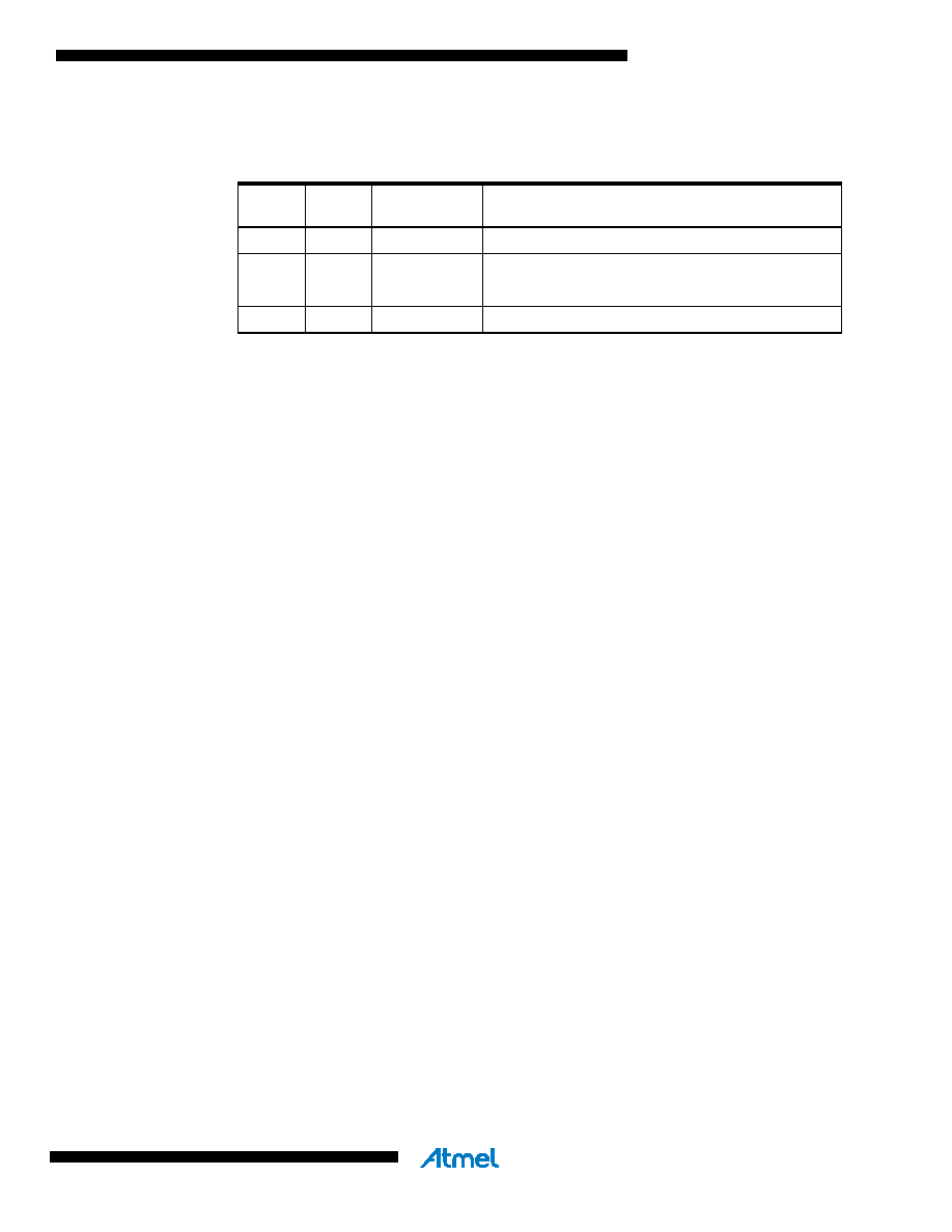
Table 6-1.
EEPROM Mode Bits
EEPM1
EEPM0
Programming
Time
Operation
0
3.4 ms
Erase and Write in one operation (Atomic Operation)
0
1
1.8 ms
Erase Only
1
0
1.8 ms
Write Only
1
–
Reserved for future use
相关PDF资料 |
PDF描述 |
|---|---|
| EP20K100BC196-3 | LOADABLE PLD, PBGA196 |
| EP20K100BI196-1 | LOADABLE PLD, PBGA196 |
| EP20K100BI196-2 | LOADABLE PLD, PBGA196 |
| EP20K100BI196-3 | LOADABLE PLD, PBGA196 |
| EP20K100BC324-1 | LOADABLE PLD, PBGA324 |
相关代理商/技术参数 |
参数描述 |
|---|---|
| EP20K100BC356-1 | 功能描述:FPGA - 现场可编程门阵列 CPLD - APEX 20K 416 Macro 252 IOs RoHS:否 制造商:Altera Corporation 系列:Cyclone V E 栅极数量: 逻辑块数量:943 内嵌式块RAM - EBR:1956 kbit 输入/输出端数量:128 最大工作频率:800 MHz 工作电源电压:1.1 V 最大工作温度:+ 70 C 安装风格:SMD/SMT 封装 / 箱体:FBGA-256 |
| EP20K100BC356-1ES | 制造商:未知厂家 制造商全称:未知厂家 功能描述:FPGA |
| EP20K100BC356-1V | 制造商:Rochester Electronics LLC 功能描述:- Bulk |
| EP20K100BC356-2 | 功能描述:FPGA - 现场可编程门阵列 CPLD - APEX 20K 416 Macro 252 IOs RoHS:否 制造商:Altera Corporation 系列:Cyclone V E 栅极数量: 逻辑块数量:943 内嵌式块RAM - EBR:1956 kbit 输入/输出端数量:128 最大工作频率:800 MHz 工作电源电压:1.1 V 最大工作温度:+ 70 C 安装风格:SMD/SMT 封装 / 箱体:FBGA-256 |
| EP20K100BC356-2ES | 制造商:未知厂家 制造商全称:未知厂家 功能描述:FPGA |
发布紧急采购,3分钟左右您将得到回复。