- 您现在的位置:买卖IC网 > PDF目录224000 > HYS72T128000EU-2.5-C2 (QIMONDA AG) 128M X 72 DDR DRAM MODULE, 0.4 ns, DMA240 PDF资料下载
参数资料
| 型号: | HYS72T128000EU-2.5-C2 |
| 厂商: | QIMONDA AG |
| 元件分类: | DRAM |
| 英文描述: | 128M X 72 DDR DRAM MODULE, 0.4 ns, DMA240 |
| 封装: | GREEN, UDIMM-240 |
| 文件页数: | 14/59页 |
| 文件大小: | 3071K |
| 代理商: | HYS72T128000EU-2.5-C2 |
第1页第2页第3页第4页第5页第6页第7页第8页第9页第10页第11页第12页第13页当前第14页第15页第16页第17页第18页第19页第20页第21页第22页第23页第24页第25页第26页第27页第28页第29页第30页第31页第32页第33页第34页第35页第36页第37页第38页第39页第40页第41页第42页第43页第44页第45页第46页第47页第48页第49页第50页第51页第52页第53页第54页第55页第56页第57页第58页第59页
HYS[64/72]T[128/256]0x0EU–[19F/1.9/25F/2.5/3S]–C2
Unbuffered DDR2 SDRAM Modules
Internet Data Sheet
Rev. 1.00, 2008-06
21
12032007-I9KE-FFWO
1)
V
DDQ = 1.8 V ± 0.1V; VDD = 1.8 V ± 0.1 V.
2) Timing that is not specified is illegal and after such an event, in order to guarantee proper operation, the DRAM must be powered down
and then restarted through the specified initialization sequence before normal operation can continue.
3) Timings are guaranteed with CK/CK differential Slew Rate of 2.0 V/ns. For DQS signals timings are guaranteed with a differential Slew
Rate of 2.0 V/ns in differential strobe mode and a Slew Rate of 1 V/ns in single ended mode.
4) The CK / CK input reference level (for timing reference to CK / CK) is the point at which CK and CK cross. The DQS / DQS, RDQS / RDQS,
input reference level is the crosspoint when in differential strobe mode.
5) Inputs are not recognized as valid until
V
REF stabilizes. During the period before VREF stabilizes, CKE = 0.2 x VDDQ is recognized as low.
6) The output timing reference voltage level is
V
TT.
7) New units, ‘
t
CK.AVG‘ and ‘nCK‘, are introduced in DDR2–667 and DDR2–800. Unit ‘tCK.AVG‘ represents the actual tCK.AVG of the input clock
under operation. Unit ‘nCK‘ represents one clock cycle of the input clock, counting the actual clock edges. Note that in DDR2–400 and
DDR2–533, ‘
t
CK‘ is used for both concepts. Example: tXP = 2 [nCK] means; if Power Down exit is registered at Tm, an Active command
may be registered at Tm + 2, even if (Tm + 2 - Tm) is 2 x
t
CK.AVG + tERR.2PER(Min).
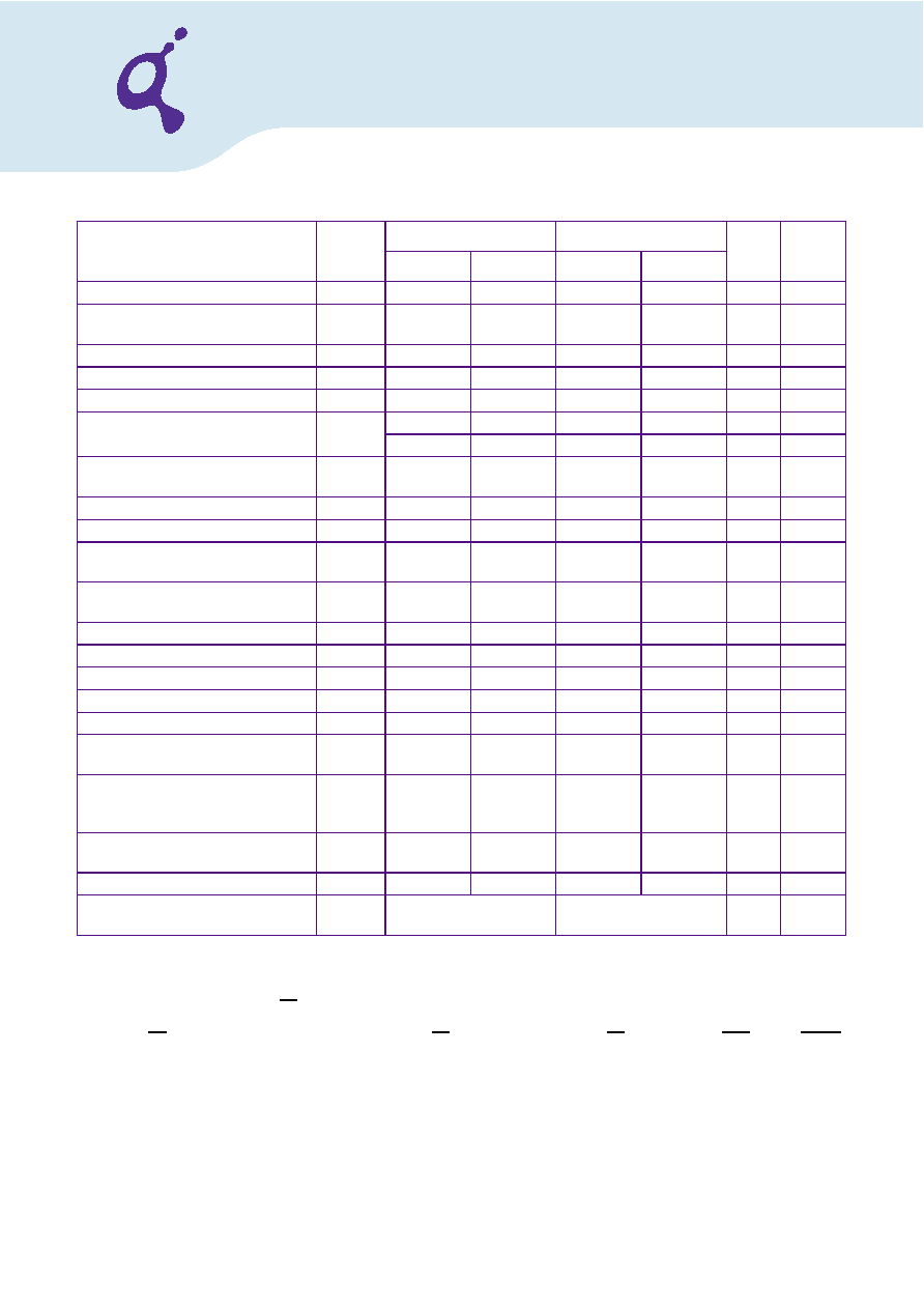
MRS command to ODT update delay
t
MOD
0
12
0
12
ns
Mode register set command cycle
time
t
MRD
2—
nCK
OCD drive mode output delay
t
OIT
0
12
0
12
ns
DQ/DQS output hold time from DQS
t
QH
t
HP – tQHS
—
t
HP – tQHS
—ps
DQ hold skew factor
t
QHS
—
300
—
340
ps
Average periodic refresh Interval
t
REFI
—7.8
μs
—3.9
μs
Auto-Refresh to Active/Auto-Refresh
command period
t
RFC
127.5
—
127.5
—
ns
Read preamble
t
RPRE
0.9
1.1
0.9
1.1
t
CK.AVG
Read postamble
t
RPST
0.4
0.6
0.4
0.6
t
CK.AVG
Active to active command period for
1KB page size products
t
RRD
7.5
—
7.5
—
ns
Internal Read to Precharge command
delay
t
RTP
7.5
—
7.5
—
ns
Write preamble
t
WPRE
0.35
—
0.35
—
t
CK.AVG
Write postamble
t
WPST
0.4
0.6
0.4
0.6
t
CK.AVG
Write recovery time
t
WR
15
—
15
—
ns
Internal write to read command delay
t
WTR
7.5
—
7.5
—
ns
Exit power down to read command
t
XARD
2—
nCK
Exit active power-down mode to read
command (slow exit, lower power)
t
XARDS
8 – AL
—
7 – AL
—
nCK
Exit precharge power-down to any
valid command (other than NOP or
Deselect)
t
XP
2—
nCK
Exit self-refresh to a non-read
command
t
XSNR
t
RFC +10
—
t
RFC +10
—
ns
Exit self-refresh to read command
t
XSRD
200
—
200
—
nCK
Write command to DQS associated
clock edges
WL
RL – 1
RL–1
nCK
Parameter
Symbol
DDR2–800
DDR2–667
Unit
Note
1)2)3
)4)5)6)7)
Min.
Max.
Min.
Max.
相关PDF资料 |
PDF描述 |
|---|---|
| HYS72T64000EP-3.7-B2 | 64M X 72 DDR DRAM MODULE, DMA240 |
| HZ20-1 | 19.25 V, 0.5 W, SILICON, UNIDIRECTIONAL VOLTAGE REGULATOR DIODE, DO-35 |
| HZ6B1L | 5.65 V, 0.4 W, SILICON, UNIDIRECTIONAL VOLTAGE REGULATOR DIODE, DO-35 |
| HZ9.1CP | 9.65 V, 1 W, SILICON, UNIDIRECTIONAL VOLTAGE REGULATOR DIODE, DO-41 |
| HZB6.8MWA | 6.8 V, 0.2 W, SILICON, UNIDIRECTIONAL VOLTAGE REGULATOR DIODE |
相关代理商/技术参数 |
参数描述 |
|---|---|
| HYS72T128000GR | 制造商:INFINEON 制造商全称:Infineon Technologies AG 功能描述:DDR2 Registered Memory Modules |
| HYS72T128000GR-37-A | 制造商:INFINEON 制造商全称:Infineon Technologies AG 功能描述:DDR2 Registered Memory Modules |
| HYS72T128000GR-5-A | 制造商:INFINEON 制造商全称:Infineon Technologies AG 功能描述:DDR2 Registered Memory Modules |
| HYS72T128000HP | 制造商:QIMONDA 制造商全称:QIMONDA 功能描述:240-Pin Registered DDR2 SDRAM Modules |
| HYS72T128000HP-2.5-B | 制造商:QIMONDA 制造商全称:QIMONDA 功能描述:240-Pin Registered DDR2 SDRAM Modules |
发布紧急采购,3分钟左右您将得到回复。