- 您现在的位置:买卖IC网 > PDF目录224000 > HYS72T128000EU-2.5-C2 (QIMONDA AG) 128M X 72 DDR DRAM MODULE, 0.4 ns, DMA240 PDF资料下载
参数资料
| 型号: | HYS72T128000EU-2.5-C2 |
| 厂商: | QIMONDA AG |
| 元件分类: | DRAM |
| 英文描述: | 128M X 72 DDR DRAM MODULE, 0.4 ns, DMA240 |
| 封装: | GREEN, UDIMM-240 |
| 文件页数: | 16/59页 |
| 文件大小: | 3071K |
| 代理商: | HYS72T128000EU-2.5-C2 |
第1页第2页第3页第4页第5页第6页第7页第8页第9页第10页第11页第12页第13页第14页第15页当前第16页第17页第18页第19页第20页第21页第22页第23页第24页第25页第26页第27页第28页第29页第30页第31页第32页第33页第34页第35页第36页第37页第38页第39页第40页第41页第42页第43页第44页第45页第46页第47页第48页第49页第50页第51页第52页第53页第54页第55页第56页第57页第58页第59页
HYS[64/72]T[128/256]0x0EU–[19F/1.9/25F/2.5/3S]–C2
Unbuffered DDR2 SDRAM Modules
Internet Data Sheet
Rev. 1.00, 2008-06
23
12032007-I9KE-FFWO
31)
t
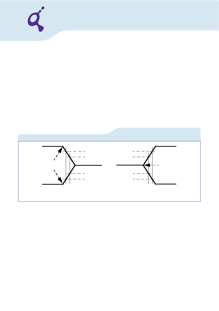
RPST end point and tRPRE begin point are not referenced to a specific voltage level but specify when the device output is no longer driving
(
t
RPST), or begins driving (tRPRE). Figure 3 shows a method to calculate these points when the device is no longer driving (tRPST), or begins
driving (
t
RPRE) by measuring the signal at two different voltages. The actual voltage measurement points are not critical as long as the
calculation is consistent.
32) When the device is operated with input clock jitter, this parameter needs to be derated by the actual
t
JIT.PER of the input clock. (output
deratings are relative to the SDRAM input clock.) For example, if the measured jitter into a DDR2–667 SDRAM has
t
JIT.PER.MIN = – 72 ps
and
t
JIT.PER.MAX = + 93 ps, then tRPRE.MIN(DERATED) = tRPRE.MIN + tJIT.PER.MIN = 0.9 x tCK.AVG – 72 ps = + 2178 ps and tRPRE.MAX(DERATED) = tRPRE.MAX
+
t
JIT.PER.MAX = 1.1 x tCK.AVG + 93 ps = + 2843 ps. (Caution on the MIN/MAX usage!).
33) When the device is operated with input clock jitter, this parameter needs to be derated by the actual
t
JIT.DUTY of the input clock. (output
deratings are relative to the SDRAM input clock.) For example, if the measured jitter into a DDR2–667 SDRAM has
t
JIT.DUTY.MIN = – 72 ps
and
t
JIT.DUTY.MAX = + 93 ps, then tRPST.MIN(DERATED) = tRPST.MIN + tJIT.DUTY.MIN = 0.4 x tCK.AVG – 72 ps = + 928 ps and tRPST.MAX(DERATED) = tRPST.MAX
+
t
JIT.DUTY.MAX = 0.6 x tCK.AVG + 93 ps = + 1592 ps. (Caution on the MIN/MAX usage!).
34) For these parameters, the DDR2 SDRAM device is characterized and verified to support
t
nPARAM = RU{tPARAM / tCK.AVG}, which is in clock
cycles, assuming all input clock jitter specifications are satisfied. For example, the device will support
t
nRP = RU{tRP / tCK.AVG}, which is in
clock cycles, if all input clock jitter specifications are met. This means: For DDR2–667 5–5–5, of which
t
RP = 15 ns, the device will support
t
nRP = RU{tRP / tCK.AVG} = 5, i.e. as long as the input clock jitter specifications are met, Precharge command at Tm and Active command at
Tm + 5 is valid even if (Tm + 5 - Tm) is less than 15 ns due to input clock jitter.
35)
t
WTR is at lease two clocks (2 x tCK) independent of operation frequency.
36) This timing parameter is relaxed than Industry Standard
FIGURE 3
Method for Calculating Transitions and Endpoint
相关PDF资料 |
PDF描述 |
|---|---|
| HYS72T64000EP-3.7-B2 | 64M X 72 DDR DRAM MODULE, DMA240 |
| HZ20-1 | 19.25 V, 0.5 W, SILICON, UNIDIRECTIONAL VOLTAGE REGULATOR DIODE, DO-35 |
| HZ6B1L | 5.65 V, 0.4 W, SILICON, UNIDIRECTIONAL VOLTAGE REGULATOR DIODE, DO-35 |
| HZ9.1CP | 9.65 V, 1 W, SILICON, UNIDIRECTIONAL VOLTAGE REGULATOR DIODE, DO-41 |
| HZB6.8MWA | 6.8 V, 0.2 W, SILICON, UNIDIRECTIONAL VOLTAGE REGULATOR DIODE |
相关代理商/技术参数 |
参数描述 |
|---|---|
| HYS72T128000GR | 制造商:INFINEON 制造商全称:Infineon Technologies AG 功能描述:DDR2 Registered Memory Modules |
| HYS72T128000GR-37-A | 制造商:INFINEON 制造商全称:Infineon Technologies AG 功能描述:DDR2 Registered Memory Modules |
| HYS72T128000GR-5-A | 制造商:INFINEON 制造商全称:Infineon Technologies AG 功能描述:DDR2 Registered Memory Modules |
| HYS72T128000HP | 制造商:QIMONDA 制造商全称:QIMONDA 功能描述:240-Pin Registered DDR2 SDRAM Modules |
| HYS72T128000HP-2.5-B | 制造商:QIMONDA 制造商全称:QIMONDA 功能描述:240-Pin Registered DDR2 SDRAM Modules |
发布紧急采购,3分钟左右您将得到回复。