- 您现在的位置:买卖IC网 > PDF目录239729 > IBM25PPC750GXEBB2532T 32-BIT, 800 MHz, RISC PROCESSOR, CBGA292 PDF资料下载
参数资料
| 型号: | IBM25PPC750GXEBB2532T |
| 元件分类: | 微控制器/微处理器 |
| 英文描述: | 32-BIT, 800 MHz, RISC PROCESSOR, CBGA292 |
| 封装: | 21 X 21 MM, 1 MM PITCH, CERAMIC, BGA-292 |
| 文件页数: | 32/74页 |
| 文件大小: | 1054K |
| 代理商: | IBM25PPC750GXEBB2532T |
第1页第2页第3页第4页第5页第6页第7页第8页第9页第10页第11页第12页第13页第14页第15页第16页第17页第18页第19页第20页第21页第22页第23页第24页第25页第26页第27页第28页第29页第30页第31页当前第32页第33页第34页第35页第36页第37页第38页第39页第40页第41页第42页第43页第44页第45页第46页第47页第48页第49页第50页第51页第52页第53页第54页第55页第56页第57页第58页第59页第60页第61页第62页第63页第64页第65页第66页第67页第68页第69页第70页第71页第72页第73页第74页
Datasheet
IBM PowerPC 750GX RISC Microprocessor
DD1.X
Dimensions and Signal Assignments
Page 38 of 73
750GX_ds_body.fm SA14-2765-02
September 2, 2005
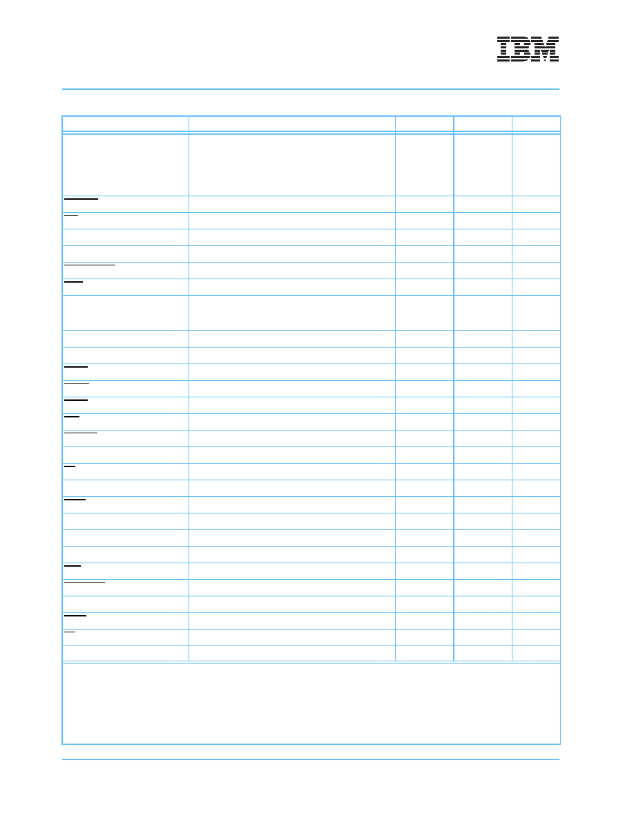
GND
B2, B19, C5, C8, C13, C16, D10, D11, E3, E7, E14,
E18, F10, F11, G5, G8, G13, G16, H3, H8, H9, H12,
H13, H18, J12, K4, K7, K10, K14, K17, L4, L7, L10,
L14, L17, M12, N3, N8, N9, N12, N13, N18, P5, P8.
P13, P16, R10, R11, T3, T7, T14, T18, U10, U11, V5,
V8, V13,V16, W2, W19,
——
HRESET
Y11
Low
Input
INT
Y9
Low
Input
L1_TSTCLK
Y13
High
Input
L2_TSTCLK
W13
High
Input
LSSD_MODE
U13
Low
Input
MCP
W12
Low
Input
OVDD
C4, C7, C14, C17, D3, D18, E10, E11, G3, G7, G14,
G18, H5, H16, K5, K16, L5, L16, N5, N16, P3, P7, P14,
P18, T10, T11, U3, U18, V4, V7, V14, V17
——
PLL_CFG[0:4]
Y18, W17, Y17, U16, W14
High
Input
PLL_RNG[0:1]
W15, U14
High
Input
QACK
Y8
Low
Input
QREQ
U8
Low
Output
RSRV
Y4
Low
Output
SMI
W10
Low
Input
SRESET
Y7
Low
Input
SYSCLK
W16
High
Input
TA
A12
Low
Input
TBEN
W8
High
Input
TBST
A11
Low
Input/Output
TCK
T2
High
Input
TDI
V2
High
Input
TDO
W5
High
Output
TEA
W6
Low
Input
TLBISYNC
W11
Low
Input
TMS
V1
High
Input
TRST
U1
Low
Input
TS
B15
Low
Input/Output
TSIZ[0:2]
A14, B12, B11
High
Output
Table 4-2. Pinout Listing for the CBGA package (Continued)
Signal Name
Pin Number
Active
Input/Output
Notes
Notes:
1. These are test signals for factory use only and must be pulled up to OVDD for normal machine operation.
2. OVDD inputs supply power to the input/output drivers and VDD inputs supply power to the processor core.
3. These pins are reserved for potential future use.
4. BVSEL and L1_TSTCLK select the input/output voltage mode on the 60x bus.
5. TCK must be tied high or low for normal machine operation.
6. Address and data parity should be left floating if unused in the design.
相关PDF资料 |
PDF描述 |
|---|---|
| ICS843023AGT | 320 MHz, OTHER CLOCK GENERATOR, PDSO8 |
| IRFR9121 | 5.9 A, 80 V, 0.6 ohm, P-CHANNEL, Si, POWER, MOSFET, TO-252AA |
| IM1P-67202AV-25 | 1K X 9 OTHER FIFO, 25 ns, CDIP28 |
| IM3P-67202AL-45 | 1K X 9 OTHER FIFO, 45 ns, PDIP28 |
| IMDP-67202AL-25 | 1K X 9 OTHER FIFO, 25 ns, CDFP28 |
相关代理商/技术参数 |
参数描述 |
|---|---|
| IBM25PPC750GXEBB2562T | 制造商:IBM 功能描述: |
| IBM25PPC750GXEBB2563T | 制造商:IBM 功能描述: |
| IBM25PPC750GXECB2563T | 制造商:IBM 功能描述: |
| IBM25PPC750GXECB2H33T | 制造商:IBM 功能描述: |
| IBM25PPC750GXECB5H42V | 制造商:IBM 功能描述:POLARIS 1.2 ? 21CBGA GRE2 ? HALFMODE 933MH - Trays |
发布紧急采购,3分钟左右您将得到回复。