- 您现在的位置:买卖IC网 > PDF目录239729 > IBM25PPC750GXEBB2532T 32-BIT, 800 MHz, RISC PROCESSOR, CBGA292 PDF资料下载
参数资料
| 型号: | IBM25PPC750GXEBB2532T |
| 元件分类: | 微控制器/微处理器 |
| 英文描述: | 32-BIT, 800 MHz, RISC PROCESSOR, CBGA292 |
| 封装: | 21 X 21 MM, 1 MM PITCH, CERAMIC, BGA-292 |
| 文件页数: | 57/74页 |
| 文件大小: | 1054K |
| 代理商: | IBM25PPC750GXEBB2532T |
第1页第2页第3页第4页第5页第6页第7页第8页第9页第10页第11页第12页第13页第14页第15页第16页第17页第18页第19页第20页第21页第22页第23页第24页第25页第26页第27页第28页第29页第30页第31页第32页第33页第34页第35页第36页第37页第38页第39页第40页第41页第42页第43页第44页第45页第46页第47页第48页第49页第50页第51页第52页第53页第54页第55页第56页当前第57页第58页第59页第60页第61页第62页第63页第64页第65页第66页第67页第68页第69页第70页第71页第72页第73页第74页
Datasheet
IBM PowerPC 750GX RISC Microprocessor
DD1.X
System Design Information
Page 60 of 73
750GX_ds_body.fm SA14-2765-02
September 2, 2005
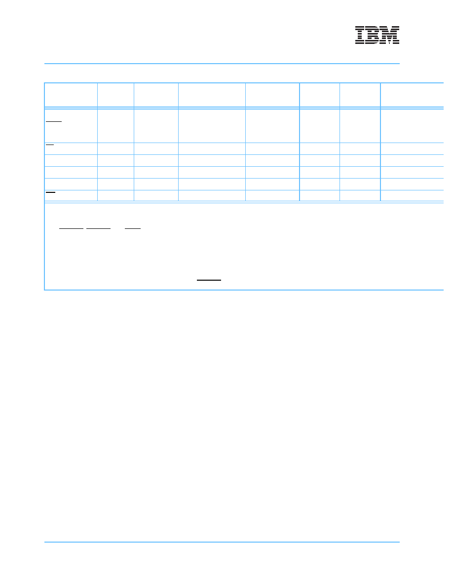
TRST
Low
Input
JTAG
Enabled high
Internal
enabled
50
a @ 2.5 V
25
a @ 1.8 V
(the pullup current for th
nal resistor)
TS
Low
Input/Output
Address Start
Keeper
5 K
Pullup required to OVDD
TSIZ[0:2]
High
Output
Transfer Attributes
Keeper
TT[0:4]
High
Input/Output
Transfer Attributes
Keeper
VDD
—
Power Supply
WT
Low
Output
Transfer Attributes
Keeper
Table 5-6. Input/Output Usage (Continued)
750GX Signal
Name
Active Level
Input/
Output
Usage Group
Input/Output with
Internal
Pullup Resistors
Level Protect
Required
External
Resistor
Comments
Notes:
1. Depends on the system design. The electrical characteristics of the 750GX do not add additional constraints to the system design, so whatever is do
depend on the system requirements.
2. HRESET, SRESET, and TRST are signals used for RISCWatch to enable proper operation of the debuggers. Logical AND gates should be placed b
and the IBM PowerPC 750GX RISC Microprocessor (see Figure 5-6 on page 61).
3. The 750GX provides protection from meta-stability on inputs through the use of a “keeper” circuit on specific inputs (see Section 5.9 on page 69 for
description).
4. If a system design requires a signal level to be maintained while not being actively driven, an external resistor or device must be used (keepers assu
inputs but do not guarantee a level).
5. The 750GX does not require external pullups on address and data lines. Control lines must be treated individually.
6. Mode Select/Control pins require the proper state at HRESET to configure the operating mode of the processor (see Table 5-10, Summary of Mode
相关PDF资料 |
PDF描述 |
|---|---|
| ICS843023AGT | 320 MHz, OTHER CLOCK GENERATOR, PDSO8 |
| IRFR9121 | 5.9 A, 80 V, 0.6 ohm, P-CHANNEL, Si, POWER, MOSFET, TO-252AA |
| IM1P-67202AV-25 | 1K X 9 OTHER FIFO, 25 ns, CDIP28 |
| IM3P-67202AL-45 | 1K X 9 OTHER FIFO, 45 ns, PDIP28 |
| IMDP-67202AL-25 | 1K X 9 OTHER FIFO, 25 ns, CDFP28 |
相关代理商/技术参数 |
参数描述 |
|---|---|
| IBM25PPC750GXEBB2562T | 制造商:IBM 功能描述: |
| IBM25PPC750GXEBB2563T | 制造商:IBM 功能描述: |
| IBM25PPC750GXECB2563T | 制造商:IBM 功能描述: |
| IBM25PPC750GXECB2H33T | 制造商:IBM 功能描述: |
| IBM25PPC750GXECB5H42V | 制造商:IBM 功能描述:POLARIS 1.2 ? 21CBGA GRE2 ? HALFMODE 933MH - Trays |
发布紧急采购,3分钟左右您将得到回复。