- 您现在的位置:买卖IC网 > PDF目录239729 > IBM25PPC750GXEBB2532T 32-BIT, 800 MHz, RISC PROCESSOR, CBGA292 PDF资料下载
参数资料
| 型号: | IBM25PPC750GXEBB2532T |
| 元件分类: | 微控制器/微处理器 |
| 英文描述: | 32-BIT, 800 MHz, RISC PROCESSOR, CBGA292 |
| 封装: | 21 X 21 MM, 1 MM PITCH, CERAMIC, BGA-292 |
| 文件页数: | 35/74页 |
| 文件大小: | 1054K |
| 代理商: | IBM25PPC750GXEBB2532T |
第1页第2页第3页第4页第5页第6页第7页第8页第9页第10页第11页第12页第13页第14页第15页第16页第17页第18页第19页第20页第21页第22页第23页第24页第25页第26页第27页第28页第29页第30页第31页第32页第33页第34页当前第35页第36页第37页第38页第39页第40页第41页第42页第43页第44页第45页第46页第47页第48页第49页第50页第51页第52页第53页第54页第55页第56页第57页第58页第59页第60页第61页第62页第63页第64页第65页第66页第67页第68页第69页第70页第71页第72页第73页第74页
Datasheet
IBM PowerPC 750GX RISC Microprocessor
DD1.X
Dimensions and Signal Assignments
Page 40 of 73
750GX_ds_body.fm SA14-2765-02
September 2, 2005
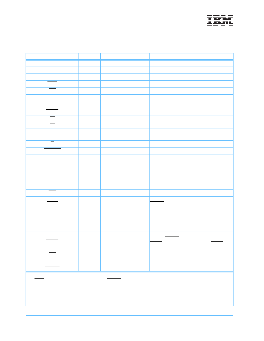
Table 4-3. Signal Listing for the CBGA Package
Signal Name
Pin Count
Active
Input/Output
Notes
A[0:31]
32
High
Input/Output
A1VDD
1
—
Supply for PLL0
A2VDD
1
—
Supply for PLL1
AACK
1
Low
Input
ABB
1
Low
Input/Output
AGND
1
—
Ground for PLL
AP[0:3]
4
High
Input/Output
ARTRY
1
Low
Input/Output
BG
1
Low
Input
BR
1
Low
Output
BVSEL
1
High
Input
I/O voltage mode select for 60x bus.
See Section 5.9.3 on page 70 for setup conditions.
CI
1
Low
Output
CKSTP_IN
1
Low
Input
CKSTP_OUT
1
Low
Output
CLK_OUT
1
High
Output
DBB
1
Low
Input/Output
DBDIS
1
Low
Input
Factory usage mode pin. Pull inactive (high) when
HRESET transitions from low to high for normal
machine operation.
DBG
1
Low
Input
DBWO
1
Low
Input
Factory usage mode pin. Pull inactive (high) when
HRESET transitions from low to high for normal
machine operation.
DH[0:31]
32
High
Input/Output
DL[0:31]
32
High
Input/Output
DP[0:31]
8
High
Input/Output
DRTRY
1
Low
Input
Optional data retry mode select. This function will be
set when HRESET transitions from low to high.
DRTRY high indicates data-retry mode; DRTRY low
indicates no data-retry mode.
GBL
1
Low
Input/Output
Ground
60
—
Common ground
HRESET
1
Low
Input
See note 1.
Notes:
1. QACK in a logical high state at the transition of HRESET from asserted to negated enables standard pre-charge mode in the
750GX.
QACK in a logical low state at the transition of HRESET from asserted to negated enables extended pre-charge mode in the
750GX.
2. QACK, in a logical low state at the transition of QREQ from asserted to negated, enables the 750GX processor to enter the soft
stop (Nap) state for proper JTAG emulator operation.
相关PDF资料 |
PDF描述 |
|---|---|
| ICS843023AGT | 320 MHz, OTHER CLOCK GENERATOR, PDSO8 |
| IRFR9121 | 5.9 A, 80 V, 0.6 ohm, P-CHANNEL, Si, POWER, MOSFET, TO-252AA |
| IM1P-67202AV-25 | 1K X 9 OTHER FIFO, 25 ns, CDIP28 |
| IM3P-67202AL-45 | 1K X 9 OTHER FIFO, 45 ns, PDIP28 |
| IMDP-67202AL-25 | 1K X 9 OTHER FIFO, 25 ns, CDFP28 |
相关代理商/技术参数 |
参数描述 |
|---|---|
| IBM25PPC750GXEBB2562T | 制造商:IBM 功能描述: |
| IBM25PPC750GXEBB2563T | 制造商:IBM 功能描述: |
| IBM25PPC750GXECB2563T | 制造商:IBM 功能描述: |
| IBM25PPC750GXECB2H33T | 制造商:IBM 功能描述: |
| IBM25PPC750GXECB5H42V | 制造商:IBM 功能描述:POLARIS 1.2 ? 21CBGA GRE2 ? HALFMODE 933MH - Trays |
发布紧急采购,3分钟左右您将得到回复。