- 您现在的位置:买卖IC网 > PDF目录20679 > ISL6329CRZ (Intersil)IC CTRLR PWM SYNC BUCK DL 60QFN PDF资料下载
参数资料
| 型号: | ISL6329CRZ |
| 厂商: | Intersil |
| 文件页数: | 18/38页 |
| 文件大小: | 0K |
| 描述: | IC CTRLR PWM SYNC BUCK DL 60QFN |
| 标准包装: | 43 |
| 应用: | 控制器,AMD SVI |
| 输入电压: | 5 V ~ 12 V |
| 输出数: | 2 |
| 输出电压: | 0.0125 V ~ 1.55 V |
| 工作温度: | 0°C ~ 70°C |
| 安装类型: | * |
| 封装/外壳: | * |
| 供应商设备封装: | * |
| 包装: | * |
第1页第2页第3页第4页第5页第6页第7页第8页第9页第10页第11页第12页第13页第14页第15页第16页第17页当前第18页第19页第20页第21页第22页第23页第24页第25页第26页第27页第28页第29页第30页第31页第32页第33页第34页第35页第36页第37页第38页
�� �
�
�ISL6329�
�or� down� to� the� appropriate� VID� level.� Finally,� the� ISL6329� will�
�then� re-enter� Power� Savings� Mode.�
�While� in� Power� Savings� Mode,� the� ISL6329� implements� two�
�features� that� effectively� enhance� the� efficiency� of� the� regulator�
�even� more.� These� features� are� Diode� Emulation� and� Gate� Voltage�
�Optimization.�
�DIODE� EMULATION�
�While� in� Power� Savings� Mode,� the� active� phases� will� behave� as� if� they�
�are� in� a� standard� buck� configuration.� To� accomplish� this,� the� lower�
�MOSFET� is� turned� on� only� while� there� is� current� flowing� to� the� load.� This�
�impedance,� the� output� voltage� under� load� can� effectively� be� level�
�shifted� down� so� that� a� larger� positive� spike� can� be� sustained� without�
�crossing� the� upper� specification� limit.�
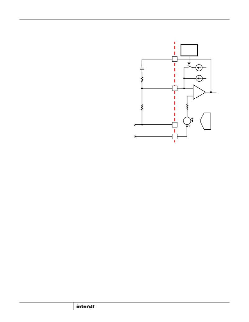
�EXTERNAL� CIRCUIT� ISL6329� INTERNAL� CIRCUIT�
�DROOP�
�CONTROL�
�COMP�
�C� C�
�I� AVG�
�behavior� emulates� the� diode� in� a� standard� buck.� The� conduction� loss�
�across� the� R� DS� (on)� of� the� MOSFET,� however,� is� much� less� than� a� diode,�
�resulting� in� a� measurable� power� savings.�
�R� C�
�FB�
�-�
�I� OFS�
�V� COMP�
�GATE� VOLTAGE� OPTIMIZATION�
�While� in� Power� Savings� Mode,� the� gate� drive� voltage� for� the� lower�
�+�
�ERROR�
�AMPLIFIER�
�MOSFETs� of� the� active� phases� is� reduced� from� the� nominal� 12V�
�that� is� utilized� in� Normal� mode� to� 5.75V.� Lowering� the� gate� drive�
�voltage� can� have� an� appreciable� effect� on� the� efficiency� of� the�
�R� FB�
�+�
�-�
�(V� DROOP� +� V� OFS� )�
�2k�
�converter.�
�In� order� to� utilize� 5V� gate� drive� at� all� times,� 5V� should� be� tied� to�
�the� PVCC� pin� and� the� GVOT� pin� should� be� shorted� to� the� PVCC�
�pin.� This� configuration� will� allow� for� 5V� gate� drive� in� all� modes� of�
�+�
�V� OUT�
�-�
�VSEN�
�RGND�
�∑�
�VID�
�DAC�
�operation.�
�V� OUT� =� V� REF� –� V� OFS� –� V� DROOP�
�V� OUT� =� V� REF� –� V� OFS� –� ?� -------------� ?� ?� K� ?� R� FB� ?�
�?� I� OUT� DCR� ?� (EQ.� 17)�
�Voltage� Regulation�
�The� integrating� compensation� network� shown� in� Figure� 8� insures�
�that� the� steady-state� error� in� the� output� voltage� is� limited� only� to�
�the� error� in� the� reference� voltage� and� offset� errors� in� the� OFS�
�current� source,� remote-sense� and� error� amplifiers.� Intersil�
�specifies� the� guaranteed� tolerance� of� the� ISL6329� to� include� the�
�combined� tolerances� of� each� of� these� elements.�
�The� output� of� the� error� amplifier,� V� COMP� ,� is� used� by� the�
�modulator� to� generate� the� PWM� signals.� The� PWM� signals�
�control� the� timing� of� the� Internal� MOSFET� drivers� and� regulate�
�the� converter� output� so� that� the� voltage� at� FB� is� equal� to� the�
�voltage� at� REF.� This� will� regulate� the� output� voltage� to� be� equal� to�
�Equation� 15.� The� internal� and� external� circuitry� that� controls�
�voltage� regulation� is� illustrated� in� Figure� 8.�
�(EQ.� 15)�
�The� ISL6329� incorporates� differential� remote-sense� amplification� in�
�the� feedback� path.� The� differential� sensing� removes� the� voltage�
�error� encountered� when� measuring� the� output� voltage� relative� to� the�
�controller� ground� reference� point� resulting� in� a� more� accurate�
�means� of� sensing� output� voltage.�
�Load-Line� (Droop)� Regulation�
�By� adding� a� well� controlled� output� impedance,� the� output� voltage�
�can� effectively� be� level� shifted� in� a� direction� which� works� to�
�achieve� a� cost-effective� solution� can� help� to� reduce� the� output-�
�voltage� spike� that� results� from� fast� load-current� demand�
�changes.�
�The� magnitude� of� the� spike� is� dictated� by� the� ESR� and� ESL� of� the� output�
�capacitors� selected.� By� positioning� the� no-load� voltage� level� near� the�
�upper� specification� limit,� a� larger� negative� spike� can� be� sustained�
�without� crossing� the� lower� limit.� By� adding� a� well� controlled� output�
�18�
�FIGURE� 8.� OUTPUT� VOLTAGE� AND� LOAD-LINE� REGULATION� WITH�
�OFFSET� ADJUSTMENT�
�As� shown� in� Figure� 8,� with� the� FS� resistor� tied� to� ground,� the�
�average� current� of� all� active� channels,� I� AVG� ,� flows� from� FB�
�through� a� load-line� regulation� resistor� R� FB� .� The� resulting� voltage�
�drop� across� R� FB� is� proportional� to� the� output� current,� effectively�
�creating� an� output� voltage� droop� with� a� steady-state� value�
�defined� as:�
�V� DROOP� =� I� AVG� ?� R� FB� (EQ.� 16)�
�The� regulated� output� voltage� is� reduced� by� the� droop� voltage�
�V� DROOP� .� The� output� voltage� as� a� function� of� load� current� is�
�shown� in� Equation� 17.�
�------------------�
�?� N� R� ISEN� ?�
�In� Equation� 17,� V� REF� is� the� reference� voltage,� V� OFS� is� the�
�programmed� offset� voltage,� I� OUT� is� the� total� output� current� of� the�
�converter,� K� is� the� DC� gain� of� the� RC� filter� across� the� inductor� (K�
�is� defined� in� Equation� 8),� N� is� the� number� of� active� channels,� and�
�DCR� is� the� distributed� inductor� impedance� value.�
�Droop� Control�
�The� DRPCTRL� (Droop� Control)� pin� is� used� to� enable� and/or�
�disable� load� line� regulation� on� both� the� Core� and� Northbridge�
�regulators.� A� single� resistor� tied� from� the� DRPCTRL� pin� to� Ground�
�will� program� the� ISL6329� to� either� enable� or� disable� droop� on�
�both� Core� and� Northbridge� simultaneously.�
�FN7800.0�
�April� 19,� 2011�
�相关PDF资料 |
PDF描述 |
|---|---|
| RSO-123.3DZ/H2 | CONV DC/DC 1W 4.5-18V +/-3.3VOUT |
| ISL6534CVZ-T | IC REG 3OUT BCK/LINEAR 24EPTSSOP |
| ASM31DRMI | CONN EDGECARD 62POS .156 SQ WW |
| GEM28DRKN | CONN EDGECARD 56POS DIP .156 SLD |
| EL7513IYZ-T13 | IC LED DRIVR WHITE BCKLGT 8-MSOP |
相关代理商/技术参数 |
参数描述 |
|---|---|
| ISL6329CRZ-T | 功能描述:电压模式 PWM 控制器 6+1 PHS DL PWM CONTRLR FOR CORE RoHS:否 制造商:Texas Instruments 输出端数量:1 拓扑结构:Buck 输出电压:34 V 输出电流: 开关频率: 工作电源电压:4.5 V to 5.5 V 电源电流:600 uA 最大工作温度:+ 125 C 最小工作温度:- 40 C 封装 / 箱体:WSON-8 封装:Reel |
| ISL6329EVAL1Z | 制造商:Intersil Corporation 功能描述:ISL6329 EVALUATION BOARD - 60 LEAD - QFN - ROHS COMPLIANT - Bulk |
| ISL6329IRZ | 功能描述:电压模式 PWM 控制器 6+1 PHS DL PWM CONTRLR FOR CORE RoHS:否 制造商:Texas Instruments 输出端数量:1 拓扑结构:Buck 输出电压:34 V 输出电流: 开关频率: 工作电源电压:4.5 V to 5.5 V 电源电流:600 uA 最大工作温度:+ 125 C 最小工作温度:- 40 C 封装 / 箱体:WSON-8 封装:Reel |
| ISL6329IRZ-T | 功能描述:电压模式 PWM 控制器 6+1 PHS DL PWM CONTRLR FOR CORE RoHS:否 制造商:Texas Instruments 输出端数量:1 拓扑结构:Buck 输出电压:34 V 输出电流: 开关频率: 工作电源电压:4.5 V to 5.5 V 电源电流:600 uA 最大工作温度:+ 125 C 最小工作温度:- 40 C 封装 / 箱体:WSON-8 封装:Reel |
| ISL6333ACRZ | 功能描述:IC CTRLR PWM 3PHASE BUCK 48-QFN RoHS:是 类别:集成电路 (IC) >> PMIC - 稳压器 - 专用型 系列:- 标准包装:43 系列:- 应用:控制器,Intel VR11 输入电压:5 V ~ 12 V 输出数:1 输出电压:0.5 V ~ 1.6 V 工作温度:-40°C ~ 85°C 安装类型:表面贴装 封装/外壳:48-VFQFN 裸露焊盘 供应商设备封装:48-QFN(7x7) 包装:管件 |
发布紧急采购,3分钟左右您将得到回复。