- 您现在的位置:买卖IC网 > PDF目录20679 > ISL6329CRZ (Intersil)IC CTRLR PWM SYNC BUCK DL 60QFN PDF资料下载
参数资料
| 型号: | ISL6329CRZ |
| 厂商: | Intersil |
| 文件页数: | 34/38页 |
| 文件大小: | 0K |
| 描述: | IC CTRLR PWM SYNC BUCK DL 60QFN |
| 标准包装: | 43 |
| 应用: | 控制器,AMD SVI |
| 输入电压: | 5 V ~ 12 V |
| 输出数: | 2 |
| 输出电压: | 0.0125 V ~ 1.55 V |
| 工作温度: | 0°C ~ 70°C |
| 安装类型: | * |
| 封装/外壳: | * |
| 供应商设备封装: | * |
| 包装: | * |
第1页第2页第3页第4页第5页第6页第7页第8页第9页第10页第11页第12页第13页第14页第15页第16页第17页第18页第19页第20页第21页第22页第23页第24页第25页第26页第27页第28页第29页第30页第31页第32页第33页当前第34页第35页第36页第37页第38页
�� �
�
�ISL6329�
�0.3�
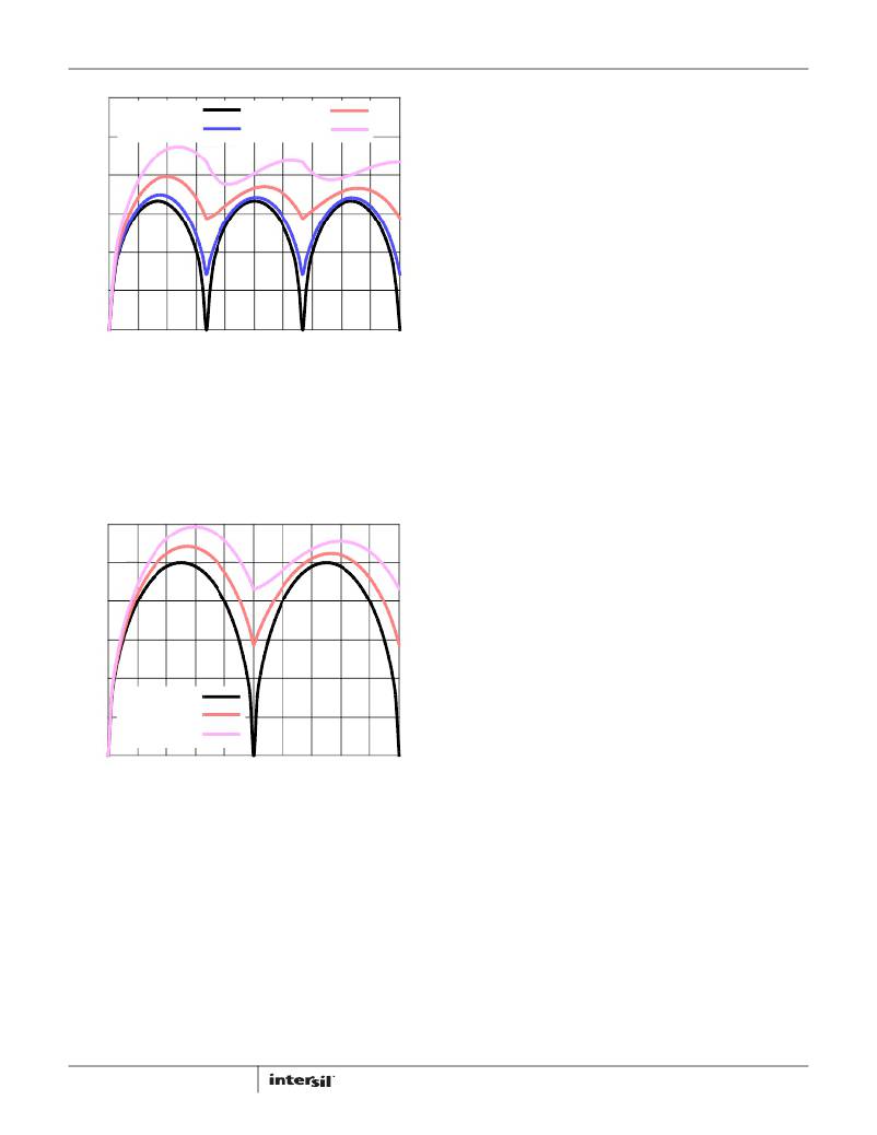
�I� L,PP� =� 0�
�I� L,PP� =� 0.25� I� O�
�I� L,PP� =� 0.5� I� O�
�I� L,PP� =� 0.75� I� O�
�Careful� component� selection,� tight� layout� of� the� critical�
�components,� and� short,� wide� circuit� traces� minimize� the�
�magnitude� of� voltage� spikes.�
�There� are� two� sets� of� critical� components� in� a� DC/DC� converter�
�using� a� ISL6329� controller.� The� power� components� are� the� most�
�0.2�
�0.1�
�0�
�0� 0.2� 0.4� 0.6� 0.8� 1.0�
�DUTY� CYCLE� (V� IN/� V� O� )�
�FIGURE� 27.� NORMALIZED� INPUT-CAPACITOR� RMS� CURRENT� FOR�
�3-PHASE� CONVERTER�
�Low� capacitance,� high-frequency� ceramic� capacitors� are� needed� in�
�addition� to� the� input� bulk� capacitors� to� suppress� leading� and�
�falling� edge� voltage� spikes.� The� spikes� result� from� the� high� current�
�slew� rate� produced� by� the� upper� MOSFET� turn� on� and� off.� Select�
�low� ESL� ceramic� capacitors� and� place� one� as� close� as� possible� to�
�each� upper� MOSFET� drain� to� minimize� board� parasitics� and�
�maximize� suppression.�
�0.3�
�0.2�
�critical� because� they� switch� large� amounts� of� energy.� Next� are�
�small� signal� components� that� connect� to� sensitive� nodes� or�
�supply� critical� bypassing� current� and� signal� coupling.�
�The� power� components� should� be� placed� first,� which� include� the�
�MOSFETs,� input� and� output� capacitors,� and� the� inductors.� It� is�
�important� to� have� a� symmetrical� layout� for� each� power� train,�
�preferably� with� the� controller� located� equidistant� from� each.�
�Symmetrical� layout� allows� heat� to� be� dissipated� equally� across� all�
�power� trains.� Equidistant� placement� of� the� controller� to� the� CORE�
�and� NB� power� trains� it� controls� through� the� integrated� drivers�
�helps� keep� the� gate� drive� traces� equally� short,� resulting� in� equal�
�trace� impedances� and� similar� drive� capability� of� all� sets� of�
�MOSFETs.�
�When� placing� the� MOSFETs,� try� to� keep� the� source� of� the� upper�
�FETs� and� the� drain� of� the� lower� FETs� as� close� as� thermally� possible.�
�Input� high-frequency� capacitors,� C� HF� ,� should� be� placed� close� to� the�
�drain� of� the� upper� FETs� and� the� source� of� the� lower� FETs.� Input�
�bulk� capacitors,� CBULK,� case� size� typically� limits� following� the�
�same� rule� as� the� high-frequency� input� capacitors.� Place� the� input�
�bulk� capacitors� as� close� to� the� drain� of� the� upper� FETs� as� possible�
�and� minimize� the� distance� to� the� source� of� the� lower� FETs.�
�Locate� the� output� inductors� and� output� capacitors� between� the�
�MOSFETs� and� the� load.� The� high-frequency� output� decoupling�
�capacitors� (ceramic)� should� be� placed� as� close� as� practicable� to� the�
�decoupling� target,� making� use� of� the� shortest� connection� paths� to�
�any� internal� planes,� such� as� vias� to� GND� next� or� on� the� capacitor�
�solder� pad.�
�The� critical� small� components� include� the� bypass� capacitors�
�0.1�
�I� L,PP� =� 0�
�I� L,PP� =� 0.5� I� O�
�(C� FILTER� )� for� VCC� and� PVCC,� and� many� of� the� components�
�surrounding� the� controller� including� the� feedback� network� and�
�current� sense� components.� Locate� the� VCC/PVCC� bypass�
�capacitors� as� close� to� the� ISL6329� as� possible.� It� is� especially�
�important� to� locate� the� components� associated� with� the�
�0�
�0�
�I� L,PP� =� 0.75� I� O�
�0.2�
�0.4�
�0.6�
�0.8�
�1.0�
�feedback� circuit� close� to� their� respective� controller� pins,� since�
�they� belong� to� a� high-impedance� circuit� loop,� sensitive� to� EMI�
�pick-up.�
�DUTY� CYCLE� (V� IN/� V� O� )�
�FIGURE� 28.� NORMALIZED� INPUT-CAPACITOR� RMS�
�CURRENT� FOR� 2-PHASE� CONVERTER�
�Layout� Considerations�
�MOSFETs� switch� very� fast� and� efficiently.� The� speed� with� which�
�the� current� transitions� from� one� device� to� another� causes� voltage�
�spikes� across� the� interconnecting� impedances� and� parasitic�
�circuit� elements.� These� voltage� spikes� can� degrade� efficiency,�
�radiate� noise� into� the� circuit� and� lead� to� device� overvoltage�
�stress.� Careful� component� selection,� layout,� and� placement�
�minimizes� these� voltage� spikes.� Consider,� as� an� example,� the�
�turnoff� transition� of� the� upper� PWM� MOSFET.� Prior� to� turnoff,� the�
�upper� MOSFET� was� carrying� channel� current.� During� the� turnoff,�
�current� stops� flowing� in� the� upper� MOSFET� and� is� picked� up� by�
�the� lower� MOSFET.� Any� inductance� in� the� switched� current� path�
�generates� a� large� voltage� spike� during� the� switching� interval.�
�34�
�A� multi-layer� printed� circuit� board� is� recommended.� Figure� 29� shows�
�the� connections� of� the� critical� components� for� the� converter.� Note�
�that� capacitors� C� IN� and� C� OUT� could� each� represent� numerous�
�physical� capacitors.� Dedicate� one� solid� layer,� usually� the� one�
�underneath� the� component� side� of� the� board,� for� a� ground� plane�
�and� make� all� critical� component� ground� connections� with� vias� to�
�this� layer.� Dedicate� another� solid� layer� as� a� power� plane� and� break�
�this� plane� into� smaller� islands� of� common� voltage� levels.� Keep� the�
�metal� runs� from� the� PHASE� terminal� to� output� inductors� short.� The�
�power� plane� should� support� the� input� power� and� output� power�
�nodes.� Use� copper� filled� polygons� on� the� top� and� bottom� circuit�
�layers� for� the� phase� nodes.� Use� the� remaining� printed� circuit� layers�
�for� small� signal� wiring.�
�FN7800.0�
�April� 19,� 2011�
�相关PDF资料 |
PDF描述 |
|---|---|
| RSO-123.3DZ/H2 | CONV DC/DC 1W 4.5-18V +/-3.3VOUT |
| ISL6534CVZ-T | IC REG 3OUT BCK/LINEAR 24EPTSSOP |
| ASM31DRMI | CONN EDGECARD 62POS .156 SQ WW |
| GEM28DRKN | CONN EDGECARD 56POS DIP .156 SLD |
| EL7513IYZ-T13 | IC LED DRIVR WHITE BCKLGT 8-MSOP |
相关代理商/技术参数 |
参数描述 |
|---|---|
| ISL6329CRZ-T | 功能描述:电压模式 PWM 控制器 6+1 PHS DL PWM CONTRLR FOR CORE RoHS:否 制造商:Texas Instruments 输出端数量:1 拓扑结构:Buck 输出电压:34 V 输出电流: 开关频率: 工作电源电压:4.5 V to 5.5 V 电源电流:600 uA 最大工作温度:+ 125 C 最小工作温度:- 40 C 封装 / 箱体:WSON-8 封装:Reel |
| ISL6329EVAL1Z | 制造商:Intersil Corporation 功能描述:ISL6329 EVALUATION BOARD - 60 LEAD - QFN - ROHS COMPLIANT - Bulk |
| ISL6329IRZ | 功能描述:电压模式 PWM 控制器 6+1 PHS DL PWM CONTRLR FOR CORE RoHS:否 制造商:Texas Instruments 输出端数量:1 拓扑结构:Buck 输出电压:34 V 输出电流: 开关频率: 工作电源电压:4.5 V to 5.5 V 电源电流:600 uA 最大工作温度:+ 125 C 最小工作温度:- 40 C 封装 / 箱体:WSON-8 封装:Reel |
| ISL6329IRZ-T | 功能描述:电压模式 PWM 控制器 6+1 PHS DL PWM CONTRLR FOR CORE RoHS:否 制造商:Texas Instruments 输出端数量:1 拓扑结构:Buck 输出电压:34 V 输出电流: 开关频率: 工作电源电压:4.5 V to 5.5 V 电源电流:600 uA 最大工作温度:+ 125 C 最小工作温度:- 40 C 封装 / 箱体:WSON-8 封装:Reel |
| ISL6333ACRZ | 功能描述:IC CTRLR PWM 3PHASE BUCK 48-QFN RoHS:是 类别:集成电路 (IC) >> PMIC - 稳压器 - 专用型 系列:- 标准包装:43 系列:- 应用:控制器,Intel VR11 输入电压:5 V ~ 12 V 输出数:1 输出电压:0.5 V ~ 1.6 V 工作温度:-40°C ~ 85°C 安装类型:表面贴装 封装/外壳:48-VFQFN 裸露焊盘 供应商设备封装:48-QFN(7x7) 包装:管件 |
发布紧急采购,3分钟左右您将得到回复。