- 您现在的位置:买卖IC网 > PDF目录16742 > ISPPAC-POWR1208-01TN44I (Lattice Semiconductor Corporation)IC ISP POWER MGR ANLG/LOG 44TQFP PDF资料下载
参数资料
| 型号: | ISPPAC-POWR1208-01TN44I |
| 厂商: | Lattice Semiconductor Corporation |
| 文件页数: | 5/35页 |
| 文件大小: | 0K |
| 描述: | IC ISP POWER MGR ANLG/LOG 44TQFP |
| 标准包装: | 160 |
| 系列: | ispPAC® |
| 应用: | 电源监控器,序列发生器 |
| 输入电压: | 0 V ~ 6 V |
| 电源电压: | 2.7 V ~ 5.5 V |
| 电流 - 电源: | 10mA |
| 工作温度: | -40°C ~ 85°C |
| 安装类型: | 表面贴装 |
| 封装/外壳: | 44-LQFP |
| 供应商设备封装: | 44-TQFP(10x10) |
| 包装: | 托盘 |
第1页第2页第3页第4页当前第5页第6页第7页第8页第9页第10页第11页第12页第13页第14页第15页第16页第17页第18页第19页第20页第21页第22页第23页第24页第25页第26页第27页第28页第29页第30页第31页第32页第33页第34页第35页
�� �
�
�Lattice� Semiconductor�
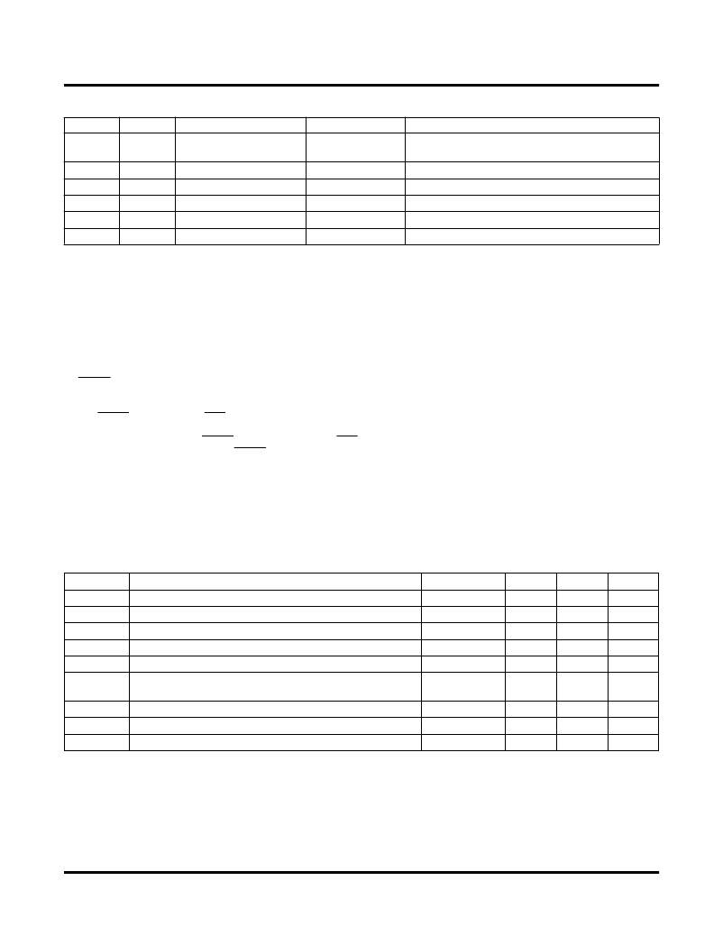
�Pin� Descriptions� (Continued)�
�ispPAC-POWR1208� Data� Sheet�
�1.17V�
�0V-5.72V�
�0V-5.72V�
�0V-5.72V�
�0V-5.72V�
�Number�
�39�
�40�
�41�
�42�
�43�
�44�
�Name�
�CREF�
�VMON8�
�VMON9�
�VMON10�
�VMON11�
�VMON12�
�Pin� Type�
�Reference�
�Analog� Input�
�Analog� Input�
�Analog� Input�
�Analog� Input�
�Analog� Input�
�Voltage� Range�
�8�
�0V-5.72V� 5�
�5�
�5�
�5�
�5�
�Description�
�Reference� for� Internal� Use,� Decoupling� Capacitor�
�(.1uf� Required,� CREF� to� GND)�
�Voltage� Monitor� Input� 8�
�Voltage� Monitor� Input� 9�
�Voltage� Monitor� Input� 10�
�Voltage� Monitor� Input� 11�
�Voltage� Monitor� Input� 12�
�1.� IN1...IN4� are� digital� inputs� to� the� PLD.� The� thresholds� for� these� pins� are� referenced� by� the� voltage� on� V� DDINP� .�
�2.� The� 18� open-drain� outputs� can� be� powered� independently� of� V� DD,� the� open-drain� outputs� can� be� pulled� up� as� high� as� +6.0V� (referenced� to�
�ground).� Exception,� CLK� pin� 26� can� only� be� pulled� as� high� as� V� DD� .�
�3.� The� four� FET� driver� outputs� (when� this� mode� is� activated,� the� corresponding� 4� open-drain� outputs� are� disabled)� are� internally� powered� and�
�can� source� up� to� 7.5V� above� V� DD� .�
�4.� V� DDINP� can� be� chosen� independent� of� V� DD.� It� applies� only� to� the� four� logic� inputs� IN1-IN4.�
�5.� The� 12� VMON� inputs� can� be� biased� independently� of� V� DD� .� The� 12� VMON� inputs� can� be� as� high� as� 7.0V� Max� (referenced� to� ground).�
�6.� CLK� is� the� PLD� clock� output� in� master� mode.� It� is� re-routed� as� an� input� in� slave� mode.� The� clock� mode� is� set� in� software� during� design� time.�
�In� output� mode� it� is� an� open-drain� type� pin� and� requires� an� external� pull-up� resistor� (pull-up� voltage� must� be� ≤� V� DD� ).� Multiple� ispPAC-�
�POWR1208� devices� can� be� tied� together� with� one� acting� as� the� master,� the� master� can� use� the� internal� clock� and� the� slave� can� be� clocked�
�by� the� master.� The� slave� needs� to� be� set� up� using� the� clock� as� an� input.�
�7.� RESET� is� an� active� low� INPUT� pin,� external� pull-up� resistor� to� V� DD� is� required.� When� driven� low� it� resets� all� internal� PLD� ?ip-?ops� to� zero� or�
�one,� and� may� turn� “ON”� or� “OFF”� the� output� pins,� including� the� HVOUT� pins� depending� on� the� polarity� con?guration� of� the� outputs� in� the�
�PLD.� If� a� reset� function� is� needed� for� the� other� devices� on� the� board,� the� PLD� inputs� and� outputs� can� be� used� to� generate� these� signals.�
�The� RESET� connected� to� the� POR� pin� can� be� used� if� multiple� ispPAC-POWR1208� devices� are� cascaded� together� in� expansion� mode� or� if�
�a� manual� reset� button� is� needed� to� reset� the� PLD� logic� to� the� i� nitial� state.� While� using� the� ispPAC-POWR1208� in� hot-swap� applications� it� is�
�recommended� that� either� the� RESET� pin� be� connected� to� the� POR� pin,� or� connect� a� capacitor� to� ground� (such� that� the� time� constant� is� 10�
�ms� with� the� pull-up� resistor)� from� the� RESET� pin.�
�8.� The� CREF� pin� requires� a� 0.1μF� capacitor� to� ground,� near� the� device� pin.� This� reference� is� used� internally� by� the� device.� No� additional� exter-�
�nal� circuitry� should� be� connected� to� this� pin.�
�Absolute� Maximum� Ratings�
�Absolute� maximum� ratings� are� shown� in� the� table� below.� Stresses� above� those� listed� values� may� cause� permanent�
�damage� to� the� device.� Functional� operation� of� the� device� at� these� or� any� other� conditions� above� those� indicated� in�
�the� operating� sections� of� this� speci?cation� is� not� implied.�
�Symbol�
�V� DD�
�Parameter�
�Core� supply� voltage� at� pin�
�Conditions�
�—�
�Min.�
�-0.5�
�Max.�
�6.0�
�Units�
�V�
�V� DDINP�
�1�
�Digital� input� supply� voltage� for� IN1-IN4�
�—�
�-0.5�
�6.0�
�V�
�HVOUTmax� HVOUT� pin� voltage,� max� =� V� DD� +� 9V�
�—�
�-0.5�
�15�
�V�
�V� IN� 2�
�VMON�
�V� TRI�
�T� S�
�T� A�
�T� SOL�
�Input� voltage� applied,� digital� inputs�
�Input� voltage� applied,� V� MON� voltage� monitor� inputs�
�Tristated� or� open� drain� output,� external� voltage� applied� (CLK�
�pin� 26� pullup� ≤� V� DD� ).�
�Storage� temperature�
�Ambient� temperature� with� power� applied�
�Maximum� soldering� temperature� (10� sec.� at� 1/16� in.)�
�—�
�—�
�—�
�—�
�—�
�—�
�-0.5�
�-0.5�
�-0.5�
�-65�
�-55�
�—�
�6.0�
�7.0�
�6.0�
�150�
�125�
�260�
�V�
�V�
�V�
�°C�
�°C�
�°C�
�1.� V� DDINP� is� the� supply� pin� that� controls� logic� inputs� IN1-IN4� only.� Place� 0.1μF� capacitor� to� ground� and� supply� the� V� DDINP� pin� with� appropriate�
�supply� voltage� for� the� given� input� logic� range.�
�2.� Digital� inputs� are� tolerant� up� to� 5.5V,� independent� of� the� V� DDINP� voltage.�
�1-4�
�相关PDF资料 |
PDF描述 |
|---|---|
| ES1000-NO.4-B7-X-75MM | HEAT SHRINK TUBING |
| EBM36DCTS | CONN EDGECARD 72POS DIP .156 SLD |
| FSLBOT | KIT TOWER MECH BOARD |
| SN65LVDS31-33EVM | EVAL MOD FOR SN65LVDS31/33 |
| 4426R-3 | INDUCTOR AIR CORE 8.0NH SMD |
相关代理商/技术参数 |
参数描述 |
|---|---|
| ISPPAC-POWR1208-01TN44I7R | 制造商:Lattice Semiconductor Corporation 功能描述: |
| ISPPAC-POWR1208P1 | 制造商:LATTICE 制造商全称:Lattice Semiconductor 功能描述:In-System Programmable Power Supply Sequencing Controller and Precision Monitor |
| ISPPACPOWR1208P101T44I | 制造商:Lattice Semiconductor Corporation 功能描述: |
| ISPPAC-POWR1208P1-01T44I | 功能描述:监控电路 PROGRAMMABLE PWR SUPPLY CONTR RoHS:否 制造商:STMicroelectronics 监测电压数: 监测电压: 欠电压阈值: 过电压阈值: 输出类型:Active Low, Open Drain 人工复位:Resettable 监视器:No Watchdog 电池备用开关:No Backup 上电复位延迟(典型值):10 s 电源电压-最大:5.5 V 最大工作温度:+ 85 C 安装风格:SMD/SMT 封装 / 箱体:UDFN-6 封装:Reel |
| ISPPAC-POWR1208P1-01TN44I | 功能描述:监控电路 PROGRAMMABLE PWR SUPPLY CONTR RoHS:否 制造商:STMicroelectronics 监测电压数: 监测电压: 欠电压阈值: 过电压阈值: 输出类型:Active Low, Open Drain 人工复位:Resettable 监视器:No Watchdog 电池备用开关:No Backup 上电复位延迟(典型值):10 s 电源电压-最大:5.5 V 最大工作温度:+ 85 C 安装风格:SMD/SMT 封装 / 箱体:UDFN-6 封装:Reel |
发布紧急采购,3分钟左右您将得到回复。