- 您现在的位置:买卖IC网 > PDF目录3960 > KMPC8360EZUAJDG (Freescale Semiconductor)IC MPU PWRQUICC II 740-TBGA PDF资料下载
参数资料
| 型号: | KMPC8360EZUAJDG |
| 厂商: | Freescale Semiconductor |
| 文件页数: | 28/95页 |
| 文件大小: | 0K |
| 描述: | IC MPU PWRQUICC II 740-TBGA |
| 标准包装: | 2 |
| 系列: | MPC83xx |
| 处理器类型: | 32-位 MPC83xx PowerQUICC II Pro |
| 速度: | 533MHz |
| 电压: | 1.2V |
| 安装类型: | 表面贴装 |
| 封装/外壳: | 740-LBGA |
| 供应商设备封装: | 740-TBGA(37.5x37.5) |
| 包装: | 托盘 |
第1页第2页第3页第4页第5页第6页第7页第8页第9页第10页第11页第12页第13页第14页第15页第16页第17页第18页第19页第20页第21页第22页第23页第24页第25页第26页第27页当前第28页第29页第30页第31页第32页第33页第34页第35页第36页第37页第38页第39页第40页第41页第42页第43页第44页第45页第46页第47页第48页第49页第50页第51页第52页第53页第54页第55页第56页第57页第58页第59页第60页第61页第62页第63页第64页第65页第66页第67页第68页第69页第70页第71页第72页第73页第74页第75页第76页第77页第78页第79页第80页第81页第82页第83页第84页第85页第86页第87页第88页第89页第90页第91页第92页第93页第94页第95页
MPC8358E PowerQUICC II Pro Processor Revision 2.1 PBGA Silicon Hardware Specifications, Rev. 3
34
Freescale Semiconductor
UCC Ethernet Controller: Three-Speed Ethernet, MII Management
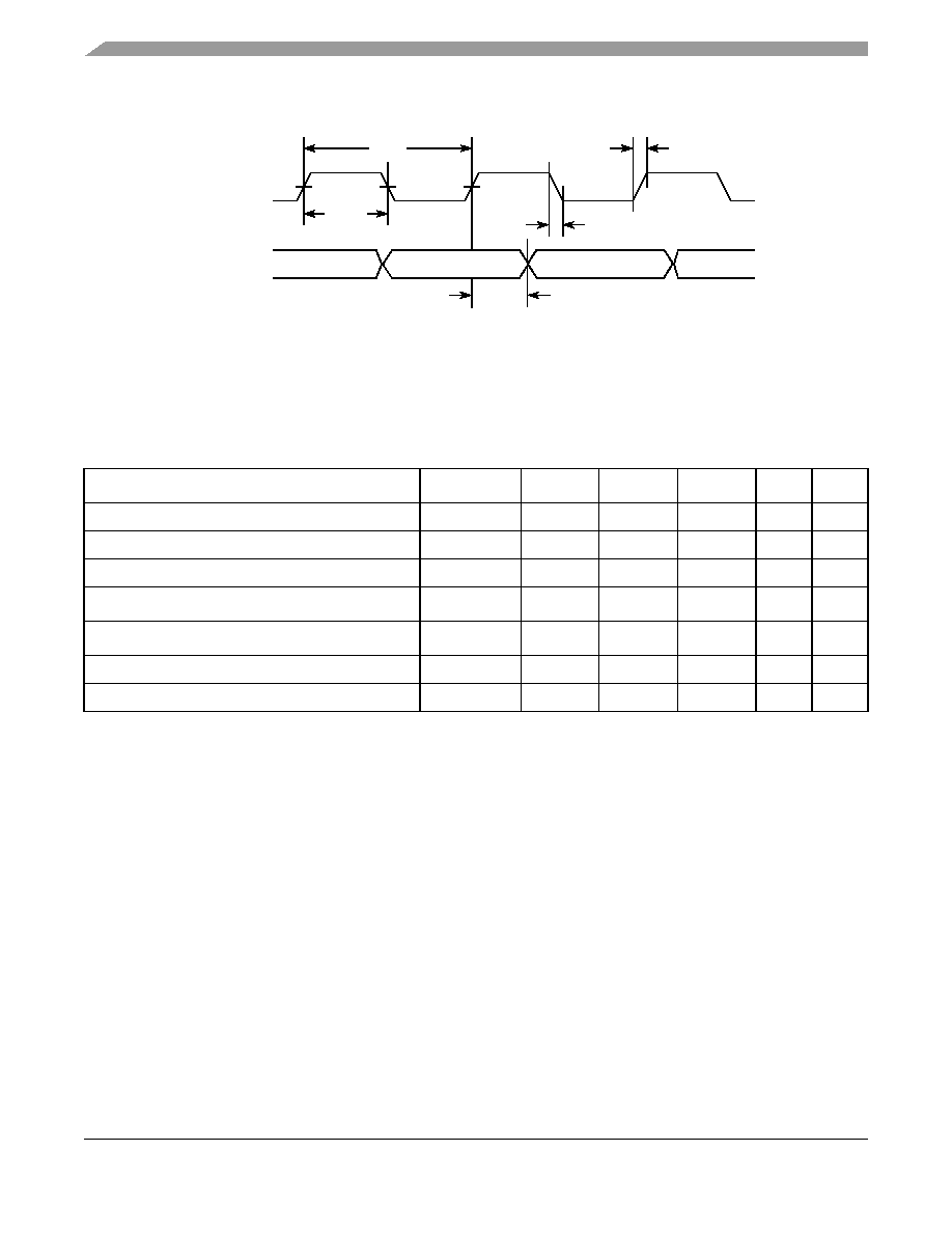
Figure 17 shows the TBI transmit AC timing diagram.
Figure 17. TBI Transmit AC Timing Diagram
8.2.4.2
TBI Receive AC Timing Specifications
Table 33 provides the TBI receive AC timing specifications.
Table 33. TBI Receive AC Timing Specifications
At recommended operating conditions with LVDD/OVDD of 3.3 V ± 10%.
Parameter/Condition
Symbol1
Min
Typ
Max
Unit
Notes
PMA_RX_CLK clock period
tTRX
—
16.0
—
ns
—
PMA_RX_CLK skew
tSKTRX
7.5
—
8.5
ns
—
RX_CLK duty cycle
tTRXH/tTRX
40
—
60
%
—
RCG[9:0] setup time to rising PMA_RX_CLK
tTRDVKH
2.5
—
ns
2
RCG[9:0] hold time to rising PMA_RX_CLK
tTRDXKH
1.0
—
ns
2
RX_CLK clock rise time, VIL(min) to VIH(max)
tTRXR
0.7
—
2.4
ns
—
RX_CLK clock fall time, VIH(max) to VIL(min)
tTRXF
0.7
—
2.4
ns
—
Notes:
1. The symbols used for timing specifications follow the pattern of t(first two letters of functional block)(signal)(state)(reference)(state) for
inputs and t(first two letters of functional block)(reference)(state)(signal)(state) for outputs. For example, tTRDVKH symbolizes TBI receive
timing (TR) with respect to the time data input signals (D) reach the valid state (V) relative to the tTRX clock reference (K)
going to the high (H) state or setup time. Also, tTRDXKH symbolizes TBI receive timing (TR) with respect to the time data input
signals (D) went invalid (X) relative to the tTRX clock reference (K) going to the high (H) state. Note that, in general, the clock
reference symbol representation is based on three letters representing the clock of a particular functional. For example, the
subscript of tTRX represents the TBI (T) receive (RX) clock. For rise and fall times, the latter convention is used with the
appropriate letter: R (rise) or F (fall). For symbols representing skews, the subscript is skew (SK) followed by the clock that
is being skewed (TRX).
2. Setup and hold time of even numbered RCG are measured from riding edge of PMA_RX_CLK1. Setup and hold time of odd
numbered RCG are measured from riding edge of PMA_RX_CLK0.
GTX_CLK
TXD[7:0]
tTTX
tTTXH
tTTXR
tTTXF
tTTKHDX
TX_EN
TX_ER
相关PDF资料 |
PDF描述 |
|---|---|
| IDT70T3319S133BFI | IC SRAM 4MBIT 133MHZ 208FBGA |
| KMPC8360EZUALFG | IC MPU PWRQUICC II 740-TBGA |
| IDT70T3319S133BFGI | IC SRAM 4MBIT 133MHZ 208FBGA |
| KMPC850DEZQ80BU | IC MPU PWRQUICC 80MHZ 256-PBGA |
| IDT70T3339S133BF8 | IC SRAM 9MBIT 133MHZ 208FBGA |
相关代理商/技术参数 |
参数描述 |
|---|---|
| KMPC8360EZUAJDGA | 功能描述:微处理器 - MPU 8360 TBGA ENCRP RoHS:否 制造商:Atmel 处理器系列:SAMA5D31 核心:ARM Cortex A5 数据总线宽度:32 bit 最大时钟频率:536 MHz 程序存储器大小:32 KB 数据 RAM 大小:128 KB 接口类型:CAN, Ethernet, LIN, SPI,TWI, UART, USB 工作电源电压:1.8 V to 3.3 V 最大工作温度:+ 85 C 安装风格:SMD/SMT 封装 / 箱体:FBGA-324 |
| KMPC8360EZUALFG | 功能描述:微处理器 - MPU 8360 TBGA ENCRP RoHS:否 制造商:Atmel 处理器系列:SAMA5D31 核心:ARM Cortex A5 数据总线宽度:32 bit 最大时钟频率:536 MHz 程序存储器大小:32 KB 数据 RAM 大小:128 KB 接口类型:CAN, Ethernet, LIN, SPI,TWI, UART, USB 工作电源电压:1.8 V to 3.3 V 最大工作温度:+ 85 C 安装风格:SMD/SMT 封装 / 箱体:FBGA-324 |
| KMPC8360EZUALFHA | 功能描述:微处理器 - MPU 8360 TBGA ENCRP RoHS:否 制造商:Atmel 处理器系列:SAMA5D31 核心:ARM Cortex A5 数据总线宽度:32 bit 最大时钟频率:536 MHz 程序存储器大小:32 KB 数据 RAM 大小:128 KB 接口类型:CAN, Ethernet, LIN, SPI,TWI, UART, USB 工作电源电压:1.8 V to 3.3 V 最大工作温度:+ 85 C 安装风格:SMD/SMT 封装 / 箱体:FBGA-324 |
| KMPC8360VVAHFH | 功能描述:微处理器 - MPU 8360 TBGA NON-ENC NO PB RoHS:否 制造商:Atmel 处理器系列:SAMA5D31 核心:ARM Cortex A5 数据总线宽度:32 bit 最大时钟频率:536 MHz 程序存储器大小:32 KB 数据 RAM 大小:128 KB 接口类型:CAN, Ethernet, LIN, SPI,TWI, UART, USB 工作电源电压:1.8 V to 3.3 V 最大工作温度:+ 85 C 安装风格:SMD/SMT 封装 / 箱体:FBGA-324 |
| KMPC8360VVAJDG | 功能描述:微处理器 - MPU 8360 TBGA NOPB RoHS:否 制造商:Atmel 处理器系列:SAMA5D31 核心:ARM Cortex A5 数据总线宽度:32 bit 最大时钟频率:536 MHz 程序存储器大小:32 KB 数据 RAM 大小:128 KB 接口类型:CAN, Ethernet, LIN, SPI,TWI, UART, USB 工作电源电压:1.8 V to 3.3 V 最大工作温度:+ 85 C 安装风格:SMD/SMT 封装 / 箱体:FBGA-324 |
发布紧急采购,3分钟左右您将得到回复。