- 您现在的位置:买卖IC网 > PDF目录177663 > LC5768VG-10F484I (LATTICE SEMICONDUCTOR CORP) PDF资料下载
参数资料
| 型号: | LC5768VG-10F484I |
| 厂商: | LATTICE SEMICONDUCTOR CORP |
| 元件分类: | PLD |
| 中文描述: | EE PLD, 10 ns, PBGA484 |
| 封装: | FBGA-484 |
| 文件页数: | 12/48页 |
| 文件大小: | 237K |
| 代理商: | LC5768VG-10F484I |
第1页第2页第3页第4页第5页第6页第7页第8页第9页第10页第11页当前第12页第13页第14页第15页第16页第17页第18页第19页第20页第21页第22页第23页第24页第25页第26页第27页第28页第29页第30页第31页第32页第33页第34页第35页第36页第37页第38页第39页第40页第41页第42页第43页第44页第45页第46页第47页第48页
Lattice Semiconductor
ispMACH 5000VG Family Data Sheet
2
Overview
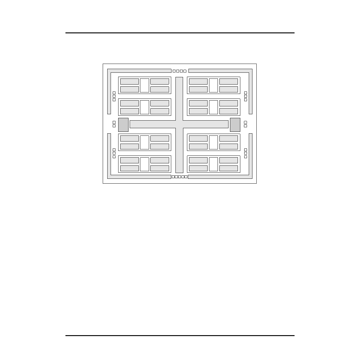
The ispMACH 5000VG devices consist of multiple SuperWIDE 68-input, 32-macrocell Generic Logic Blocks
(GLBs) interconnected by a tiered routing system. Figure 1 shows the functional block diagram of the ispMACH
5000VG. Groups of four GLBs, referred to as segments, are interconnected via a Segment Routing Pool (SRP).
Segments are interconnected via the Global Routing Pool (GRP.) Together the GLBs and the routing pools allow
designers to create large designs in a single device without compromising performance.
Each GLB has 68 inputs coming from the SRP and contains 163 product terms. These product terms form groups
of ve product term clusters, which feed the PT sharing array or the macrocell directly. The ispMACH 5000VG
allows up to 160 product terms to be connected to a single macrocell via the product term expanders and PT Shar-
ing Array.
The macrocell is designed to provide exible clocking and control functionality with the capability to select between
global, product term and block-level resources. The outputs of the macrocells are fed back into the switch matrices
and, if required, the sysIO cell.
All I/Os in the ispMACH 5000VG family are sysIOs, which are split into four banks. Each bank has a separate I/O
power supply and reference voltage. The sysIO cells allow operation with a wide range of today’s emerging inter-
face standards. Within a bank, inputs can be set to a variety of standards, providing the reference voltage require-
ments of the chosen standards are compatible. Within a bank, the outputs can be set to differing standards,
providing the I/O power supply voltage and the reference voltage requirements of the chosen standard are compat-
ible. Support for this wide range of standards allows designers to achieve signicantly higher board-level perfor-
mance compared to the more traditional LVCMOS standards.
Figure 1. Functional Block Diagram
PLL0
PLL1
GLB
VCCP0
VCCO0
GCLK0
VREF0
RESETB
GOE1
GOE2
TO
E
TDI
TDO
TMS
TCK
V
CCJ
I/O Bank 0
I/O Bank 3
I/O Bank 1
I/O Bank 2
GNDP0
VCCP1
GNDP1
GLB
Global Routing Pool
SRP
VCCO1
GCLK1
VREF1
VCCO3
GCLK3
VREF3
VCCO2
GCLK2
VREF2
GLB
相关PDF资料 |
PDF描述 |
|---|---|
| LC51024VG-10F484C | |
| LC5768VG-12F484I | |
| LC5768VG-12F256I | |
| LC5512B-75F256C | |
| LC5256B-75T128I | |
相关代理商/技术参数 |
参数描述 |
|---|---|
| LC5768VG-12F256I | 功能描述:CPLD - 复杂可编程逻辑器件 PROGRAM EXPANDED LOG RoHS:否 制造商:Lattice 系列: 存储类型:EEPROM 大电池数量:128 最大工作频率:333 MHz 延迟时间:2.7 ns 可编程输入/输出端数量:64 工作电源电压:3.3 V 最大工作温度:+ 90 C 最小工作温度:0 C 封装 / 箱体:TQFP-100 |
| LC5768VG-12F484I | 功能描述:CPLD - 复杂可编程逻辑器件 PROGRAM EXPANDED LOG RoHS:否 制造商:Lattice 系列: 存储类型:EEPROM 大电池数量:128 最大工作频率:333 MHz 延迟时间:2.7 ns 可编程输入/输出端数量:64 工作电源电压:3.3 V 最大工作温度:+ 90 C 最小工作温度:0 C 封装 / 箱体:TQFP-100 |
| LC5768VG-5F256C | 功能描述:CPLD - 复杂可编程逻辑器件 PROGRAM EXPANDED LOG RoHS:否 制造商:Lattice 系列: 存储类型:EEPROM 大电池数量:128 最大工作频率:333 MHz 延迟时间:2.7 ns 可编程输入/输出端数量:64 工作电源电压:3.3 V 最大工作温度:+ 90 C 最小工作温度:0 C 封装 / 箱体:TQFP-100 |
| LC5768VG-5F484C | 功能描述:CPLD - 复杂可编程逻辑器件 PROGRAM EXPANDED LOG RoHS:否 制造商:Lattice 系列: 存储类型:EEPROM 大电池数量:128 最大工作频率:333 MHz 延迟时间:2.7 ns 可编程输入/输出端数量:64 工作电源电压:3.3 V 最大工作温度:+ 90 C 最小工作温度:0 C 封装 / 箱体:TQFP-100 |
| LC5768VG-5FN484C | 制造商:Lattice Semiconductor Corporation 功能描述:CPLD ispMACH 5000VG Family 768 Macro Cells 178.6MHz 3.3V 484-Pin FBGA |
发布紧急采购,3分钟左右您将得到回复。