- 您现在的位置:买卖IC网 > PDF目录177663 > LC5768VG-10F484I (LATTICE SEMICONDUCTOR CORP) PDF资料下载
参数资料
| 型号: | LC5768VG-10F484I |
| 厂商: | LATTICE SEMICONDUCTOR CORP |
| 元件分类: | PLD |
| 中文描述: | EE PLD, 10 ns, PBGA484 |
| 封装: | FBGA-484 |
| 文件页数: | 45/48页 |
| 文件大小: | 237K |
| 代理商: | LC5768VG-10F484I |
第1页第2页第3页第4页第5页第6页第7页第8页第9页第10页第11页第12页第13页第14页第15页第16页第17页第18页第19页第20页第21页第22页第23页第24页第25页第26页第27页第28页第29页第30页第31页第32页第33页第34页第35页第36页第37页第38页第39页第40页第41页第42页第43页第44页当前第45页第46页第47页第48页
Lattice Semiconductor
ispMACH 5000VG Family Data Sheet
6
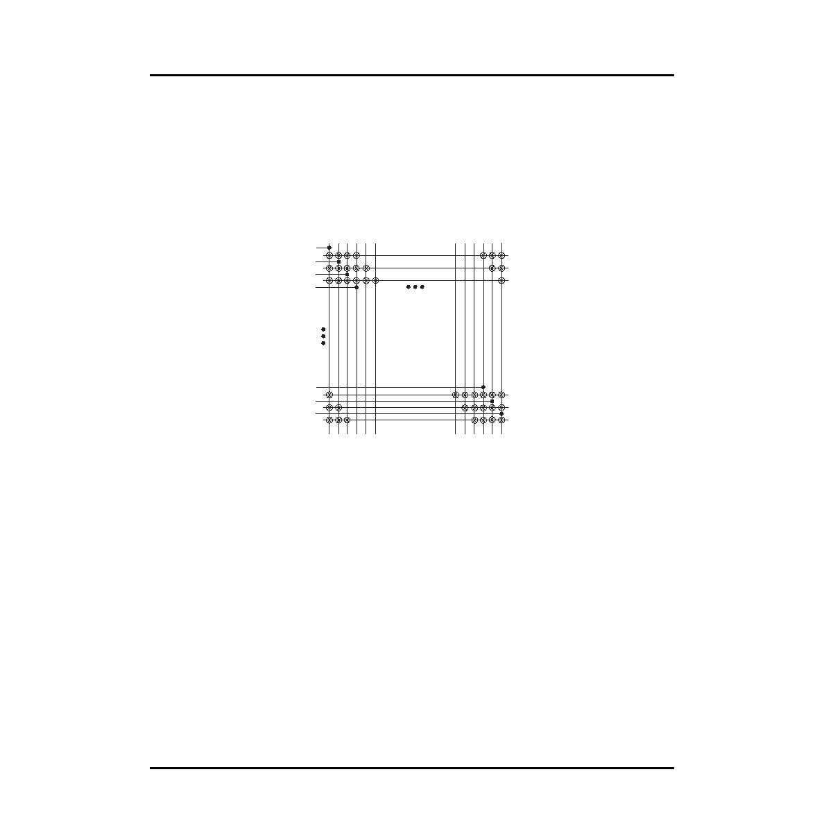
Product Term Sharing Array
The Product Term Sharing Array (PTSA) consists of 32 inputs from the Dual-OR Array (Expandable PTSA OR) and
32 outputs directly to the macrocells. Each output is the OR term of any combination of the seven Expandable
PTSA OR terms connected to that output. Every Nth macrocell is connected to N-3, N-2, N-1, N, N+1, N+2 and
N+3 PTSA OR terms via a programmable connection. This wraps around the logic, Macrocell 0 gets its logic from
29, 30, 31, 0, 1, 2, 3. The Expandable PTSA OR used in conjunction with the PTSA allows wide functions to be
implemented easily and efciently. Without using the Expandable PTSA OR capability, the greatest number of
product terms that can be included in a single function with one pass of delay is 35. Figure 6 shows the graphical
representation of the PTSA.
Macrocell
The 32 registered macrocells in the GLB are driven by the 32 outputs from the PTSA or the PTSA bypass. Each
macrocell contains a programmable XOR gate, a programmable register/latch ip-op and the necessary clocks
and control logic to allow combinatorial or registered operation.
The macrocells each have two outputs, which can be fed to the SRP, GRP and I/O cell. This dual or concurrent out-
put capability from the macrocell gives efcient use of the hardware resources. One output can be a registered
function for example, while the other output can be an unrelated combinatorial function. A direct register input from
the I/O cell facilitates efcient use of the macrocell to construct high-speed input registers.
Macrocell registers can be clocked from one of several global or product term clocks available on the device. A glo-
bal and product term clock enable is also provided, eliminating the need to gate the clock to the macrocell registers
directly. Reset and preset for the macrocell register is provided from both global and product term signals. The
macrocell register can be programmed to operate as a D-type register or a D-type latch. Figure 7 is a graphical rep-
resentation of the ispMACH 5000VG macrocell.
Figure 6. Product Term Sharing Array
PTSA OR 0
PTSA OR 1
PTSA OR 2
PTSA OR 3
PTSA OR 29
PTSA OR 30
PTSA OR 31
Macrocell 0
Macrocell 1
Macrocell 2
Macrocell 29
Macrocell 30
Macrocell 31
相关PDF资料 |
PDF描述 |
|---|---|
| LC51024VG-10F484C | |
| LC5768VG-12F484I | |
| LC5768VG-12F256I | |
| LC5512B-75F256C | |
| LC5256B-75T128I | |
相关代理商/技术参数 |
参数描述 |
|---|---|
| LC5768VG-12F256I | 功能描述:CPLD - 复杂可编程逻辑器件 PROGRAM EXPANDED LOG RoHS:否 制造商:Lattice 系列: 存储类型:EEPROM 大电池数量:128 最大工作频率:333 MHz 延迟时间:2.7 ns 可编程输入/输出端数量:64 工作电源电压:3.3 V 最大工作温度:+ 90 C 最小工作温度:0 C 封装 / 箱体:TQFP-100 |
| LC5768VG-12F484I | 功能描述:CPLD - 复杂可编程逻辑器件 PROGRAM EXPANDED LOG RoHS:否 制造商:Lattice 系列: 存储类型:EEPROM 大电池数量:128 最大工作频率:333 MHz 延迟时间:2.7 ns 可编程输入/输出端数量:64 工作电源电压:3.3 V 最大工作温度:+ 90 C 最小工作温度:0 C 封装 / 箱体:TQFP-100 |
| LC5768VG-5F256C | 功能描述:CPLD - 复杂可编程逻辑器件 PROGRAM EXPANDED LOG RoHS:否 制造商:Lattice 系列: 存储类型:EEPROM 大电池数量:128 最大工作频率:333 MHz 延迟时间:2.7 ns 可编程输入/输出端数量:64 工作电源电压:3.3 V 最大工作温度:+ 90 C 最小工作温度:0 C 封装 / 箱体:TQFP-100 |
| LC5768VG-5F484C | 功能描述:CPLD - 复杂可编程逻辑器件 PROGRAM EXPANDED LOG RoHS:否 制造商:Lattice 系列: 存储类型:EEPROM 大电池数量:128 最大工作频率:333 MHz 延迟时间:2.7 ns 可编程输入/输出端数量:64 工作电源电压:3.3 V 最大工作温度:+ 90 C 最小工作温度:0 C 封装 / 箱体:TQFP-100 |
| LC5768VG-5FN484C | 制造商:Lattice Semiconductor Corporation 功能描述:CPLD ispMACH 5000VG Family 768 Macro Cells 178.6MHz 3.3V 484-Pin FBGA |
发布紧急采购,3分钟左右您将得到回复。