- 您现在的位置:买卖IC网 > PDF目录177663 > LC5768VG-10F484I (LATTICE SEMICONDUCTOR CORP) PDF资料下载
参数资料
| 型号: | LC5768VG-10F484I |
| 厂商: | LATTICE SEMICONDUCTOR CORP |
| 元件分类: | PLD |
| 中文描述: | EE PLD, 10 ns, PBGA484 |
| 封装: | FBGA-484 |
| 文件页数: | 9/48页 |
| 文件大小: | 237K |
| 代理商: | LC5768VG-10F484I |
第1页第2页第3页第4页第5页第6页第7页第8页当前第9页第10页第11页第12页第13页第14页第15页第16页第17页第18页第19页第20页第21页第22页第23页第24页第25页第26页第27页第28页第29页第30页第31页第32页第33页第34页第35页第36页第37页第38页第39页第40页第41页第42页第43页第44页第45页第46页第47页第48页
Lattice Semiconductor
ispMACH 5000VG Family Data Sheet
17
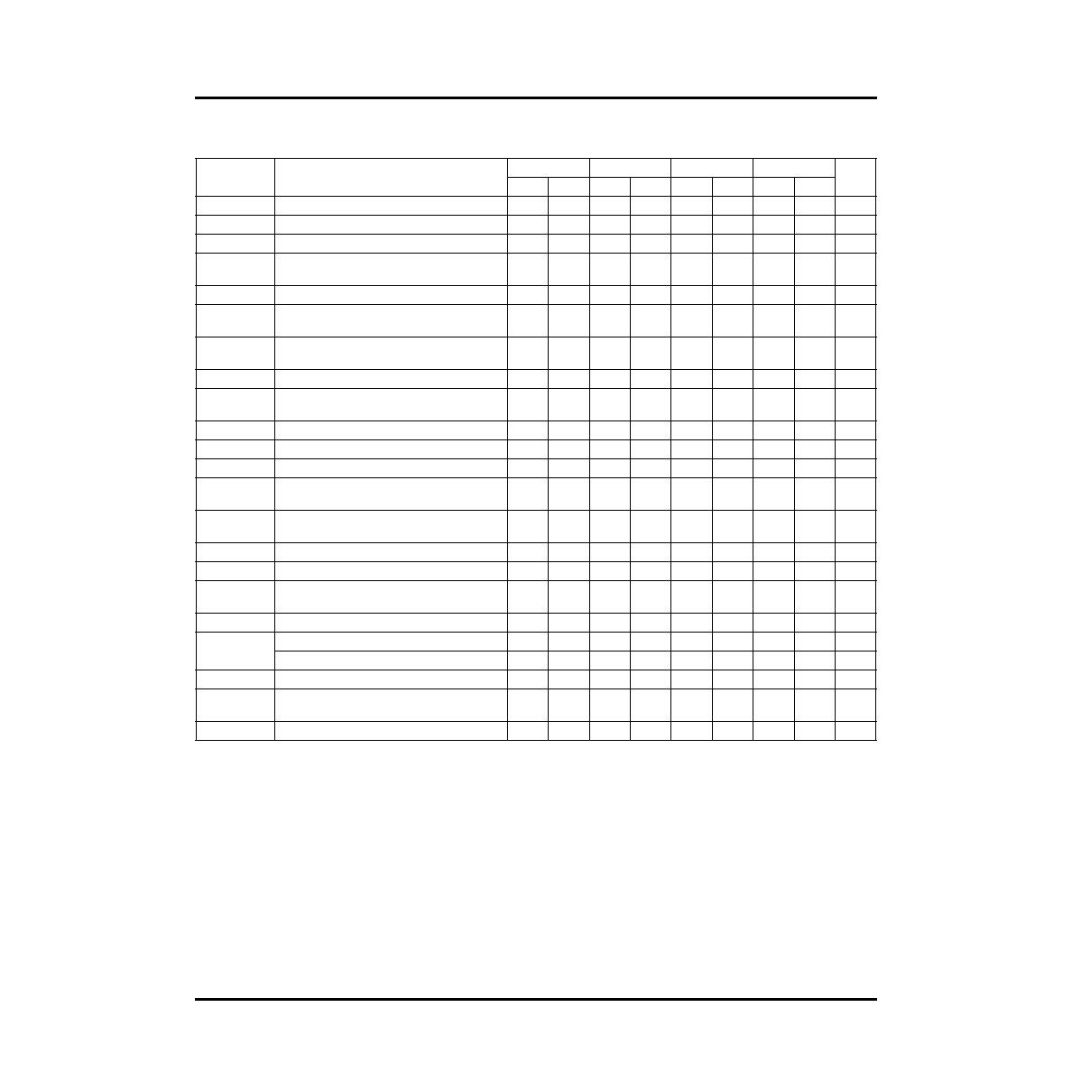
ispMACH 51024VG External Switching Characteristics
Over Recommended Operating Conditions
Parameter
Description
1,2,3
-5
-75
-10
-12
Units
Min
Max
Min
Max
Min
Max
Min
Max
tPD
Data propagation delay, 5-PT bypass
—
5.0
—
7.5
—
10.0
—
12.0
ns
tPD_PTSA
Data propagation delay, intrasegment path
—
6.0
—
9.0
—
11.5
—
13.5
ns
tPD_GLOBAL
Data propagation delay, intersegment path
—
6.5
—
9.75
—
13.0
—
16.0
ns
tS
GLB register setup time before clock,
5-PT bypass
3.0
—
5.0
—
7.5
—
9.3
—
ns
tS_PTSA
GLB register setup time before clock
3.0
—
6.0
—
8.5
—
10.0
—
ns
tSIR
GLB register setup time before clock, input
register path
2.8
—
3.0
—
4.0
—
5.0
—
ns
tH
GLB register hold time before clock, 5-PT
bypass
0.0
—
0.0
—
0.0
—
0.0
—
ns
tH_PTSA
GLB register hold time before clock
0.0
—
0.0
—
0.0
—
0.0
—
ns
tHIR
GLB register hold time before clock, input
reg. path
0.0
—
0.0
—
0.0
—
0.0
—
ns
tCO
GLB register clock-to-output delay
—
4.4
—
5.0
—
6.0
—
7.0
ns
tR
External reset pin to output delay
—
6.5
—
9.0
—
10.0
—
10.9
ns
tRW
External reset pulse duration
4.0
—
6.0
—
8.0
—
9.5
—
ns
tLPTOE/DIS
Input to output local product term output
enable/disable
—
7.0
—
9.75
—
11.5
—
13.4
ns
tSPTOE/DIS
Input to output segment product term
output enable/disable
—
8.0
—
11.25
—
17.5
—
20.4
ns
tGOE/DIS
Global OE input to output enable/disable
—
6.2
—
7.5
—
8.85
—
10.0
ns
tCW
Global clock width, high or low
1.6
—
2.75
—
3.6
—
4.3
—
ns
tGW
Global gate width low (for low transparent)
or high (for high transparent)
1.8
—
2.75
—
3.6
—
4.3
—
ns
tWIR
Input register clock width, high or low
1.8
—
2.75
—
3.6
—
4.3
—
ns
tSKEW
Clock-to-out skew, block level
—
0.25
—
0.35
—
0.45
—
0.55
ns
Clock-to-out skew, segment level
—
0.4
—
0.5
—
0.6
—
0.7
ns
fMAX
4
Clock frequency with internal feedback
178.6
—
117.0
—
87.0
—
73.0
—
MHz
fMAX (Ext.)
Clock frequency with external feedback,
1/ (tS_PTSA + tCO)
135.1
—
90.9
—
69.0
—
58.8
—
MHz
fMAX (Tog.)
Clock frequency max Toggle
312.5
—
181.0
—
138.0
—
116.0
—
MHz
Timing v.1.10
1. Timing numbers are based on default LVCMOS 3.3 I/O Buffers. Use timing adjusters provided to calculate timing for other standards.
2. Measured using standard switching circuit, assuming segment and global routing loading of 1, worst case PTSA loading and 1 output
switching.
3. Pulse widths and clock widths less than minimum will cause unknown behavior.
4. Standard 16-bit counter using SRP feedback.
相关PDF资料 |
PDF描述 |
|---|---|
| LC51024VG-10F484C | |
| LC5768VG-12F484I | |
| LC5768VG-12F256I | |
| LC5512B-75F256C | |
| LC5256B-75T128I | |
相关代理商/技术参数 |
参数描述 |
|---|---|
| LC5768VG-12F256I | 功能描述:CPLD - 复杂可编程逻辑器件 PROGRAM EXPANDED LOG RoHS:否 制造商:Lattice 系列: 存储类型:EEPROM 大电池数量:128 最大工作频率:333 MHz 延迟时间:2.7 ns 可编程输入/输出端数量:64 工作电源电压:3.3 V 最大工作温度:+ 90 C 最小工作温度:0 C 封装 / 箱体:TQFP-100 |
| LC5768VG-12F484I | 功能描述:CPLD - 复杂可编程逻辑器件 PROGRAM EXPANDED LOG RoHS:否 制造商:Lattice 系列: 存储类型:EEPROM 大电池数量:128 最大工作频率:333 MHz 延迟时间:2.7 ns 可编程输入/输出端数量:64 工作电源电压:3.3 V 最大工作温度:+ 90 C 最小工作温度:0 C 封装 / 箱体:TQFP-100 |
| LC5768VG-5F256C | 功能描述:CPLD - 复杂可编程逻辑器件 PROGRAM EXPANDED LOG RoHS:否 制造商:Lattice 系列: 存储类型:EEPROM 大电池数量:128 最大工作频率:333 MHz 延迟时间:2.7 ns 可编程输入/输出端数量:64 工作电源电压:3.3 V 最大工作温度:+ 90 C 最小工作温度:0 C 封装 / 箱体:TQFP-100 |
| LC5768VG-5F484C | 功能描述:CPLD - 复杂可编程逻辑器件 PROGRAM EXPANDED LOG RoHS:否 制造商:Lattice 系列: 存储类型:EEPROM 大电池数量:128 最大工作频率:333 MHz 延迟时间:2.7 ns 可编程输入/输出端数量:64 工作电源电压:3.3 V 最大工作温度:+ 90 C 最小工作温度:0 C 封装 / 箱体:TQFP-100 |
| LC5768VG-5FN484C | 制造商:Lattice Semiconductor Corporation 功能描述:CPLD ispMACH 5000VG Family 768 Macro Cells 178.6MHz 3.3V 484-Pin FBGA |
发布紧急采购,3分钟左右您将得到回复。