- 您现在的位置:买卖IC网 > PDF目录2082 > LMK04010BISQ/NOPB (National Semiconductor)IC CLOCK CONDITIONER W/PLL 48LLP PDF资料下载
参数资料
| 型号: | LMK04010BISQ/NOPB |
| 厂商: | National Semiconductor |
| 文件页数: | 25/65页 |
| 文件大小: | 0K |
| 描述: | IC CLOCK CONDITIONER W/PLL 48LLP |
| 标准包装: | 1,000 |
| 系列: | PowerWise® |
| 类型: | 时钟调节器 |
| PLL: | 是 |
| 输入: | LVCMOS |
| 输出: | 2VPECL,LVPECL |
| 电路数: | 1 |
| 比率 - 输入:输出: | 2:5 |
| 差分 - 输入:输出: | 是/是 |
| 频率 - 最大: | 1.296GHz |
| 除法器/乘法器: | 是/是 |
| 电源电压: | 3.15 V ~ 3.45 V |
| 工作温度: | -40°C ~ 85°C |
| 安装类型: | 表面贴装 |
| 封装/外壳: | 48-WFQFN 裸露焊盘 |
| 供应商设备封装: | 48-LLP(7x7) |
| 包装: | 带卷 (TR) |
| 其它名称: | LMK04010BISQ |
第1页第2页第3页第4页第5页第6页第7页第8页第9页第10页第11页第12页第13页第14页第15页第16页第17页第18页第19页第20页第21页第22页第23页第24页当前第25页第26页第27页第28页第29页第30页第31页第32页第33页第34页第35页第36页第37页第38页第39页第40页第41页第42页第43页第44页第45页第46页第47页第48页第49页第50页第51页第52页第53页第54页第55页第56页第57页第58页第59页第60页第61页第62页第63页第64页第65页
SNOSAZ8J – SEPTEMBER 2008 – REVISED SEPTEMBER 2011
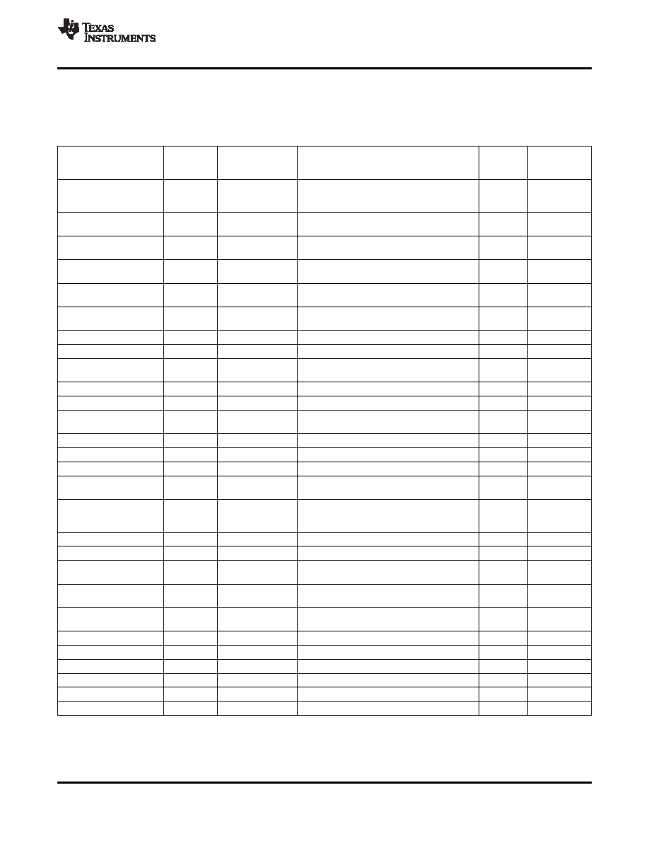
Default Device Register Settings After Power On/Reset
Table 4 illustrates the default register settings programmed in silicon for the LMK040xx after power on or
asserting the reset bit.
Table 4. Default Device Register Settings after Power On/Reset
Field Name
Default
Default State
Field Description
Register
Bit Location
Value
(MSB:LSB)
(decimal)
CLKoutX_PECL_LVL
0
2VPECL disabled
This bit sets LVPECL clock level. Valid when
R0 to R4
23
the clock channel is configured as
LVPECL/2VPECL; otherwise, not relevant.
CLKoutXB_STATE
0
Inverted
This field sets the state of output B of an
R1 to R3
22:21
LVCMOS Clock channel.
CLKoutXA_STATE
1
Non-Inverted
This field sets the state of output A of an
R1 to R3
20:19
LVCMOS Clock channel.
EN_CLKoutX
0
OFF
Clock Channel enable bit. Note: The state of
R0 to R4
16
CLKout2 is ON by default.
Reserved Registers
(1)
R5,R6,R8
NA
R9,R10
RC_DLD1_Start
1
Enabled
Forces the VCO tuning algorithm state
R10
29
machine to wait until PLL1 is locked.
CLKin1_BUFTYPE
1
MOS mode
CLKin1 Input Buffer Type
R11
11
CLKin0_BUFTYPE
1
MOS mode
CLKin0 Input Buffer Type
R11
10
LOS_TIMEOUT
1
3 MHz (min.)
Selects Lower Reference Clock input
R11
9:8
frequency for LOS Detection.
LOS_TYPE
3
CMOS
Selects LOS output type (2)
R11
7:6
CLKin_SEL
0
CLKin0
Selects Reference Clock source
R11
5:4
PLL1 CP Polarity
1
Positive polarity
Selects the charge pump output polarity, i.e.,
R12
31
the tuning slope of the external VCXO
PLL1_CP_GAIN
6
100 A
Sets the PLL1 Charge Pump Gain
R12
30:28
PLL1_R Counter
1
Divide = 1
Sets divide value for PLL1_R Counter
R12
27:16
PLL1_N Counter
1
Divide = 1
Sets divide value for PLL1_N Counter
R12
15:4
EN_PLL2_REF2X
0
Disabled
Enables or disables the OSCin frequency
R13
16
doubler path for the PLL2 reference input
EN_PLL2_XTAL
0
OFF
Enables or Disables internal circuits that
R13
21
support an external crystal driving the OSCin
pins
EN_Fout
0
OFF
Enables or disables the VCO output buffer
R13
20
CLK Global Enable
1
Enabled
Global enable or disable for output clocks
R13
18
POWER DOWN
0
Disabled (device is Device power down control
R13
17
active)
PLL2 CP TRI-STATE
0
TRI-STATE
Enables or disables TRI-STATE for PLL2
R13
15
disabled
Charge Pump
PLL1 CP TRI-STATE
0
TRI-STATE
Enables or disables TRI-STATE for PLL1
R13
14
disabled
Charge Pump
OSCin_FREQ
200
200 MHz
Source frequency driving OSCin port
R14
28:21
PLL_MUX
31
Reserved
Selects output routed to LD pin
R14
20:16
PLL2_R Counter
1
Divide = 1
Sets Divide value for PLL2_R Counter
R14
15:4
PLL2_CP_GAIN
2
1600 A
Sets PLL2 Charge Pump Gain
R15
27:26
VCO_DIV
2
Divide = 2
Sets divide value for VCO output divider
R15
25:22
PLL2_N Counter
1
Divide = 1
Sets PLL2_N Counter value
R15
21:4
(1)
These registers are reserved. The Power On/Reset values for these registers are shown in the register map and should not be changed
during programming.
(2)
If the CLKin_SEL value is set to either [0,0] or [0,1], the LOS_TYPE field should be set to [0,0].
Copyright 2008–2011, Texas Instruments Incorporated
31
相关PDF资料 |
PDF描述 |
|---|---|
| LMV393MUTAG | IC OP AMP DUAL GP LV LV 8-UDFN |
| LMX339HASD+T | IC COMPARATOR GP QUAD 14-SOIC |
| LT1011AIS8#TRPBF | IC VOLTAGE COMPARATOR 5V 8-SOIC |
| LT1016IS8#TRPBF | IC COMPARATOR 10NS HI-SPD 8-SOIC |
| LT1017IS8#TRPBF | IC COMPARATOR MICRPWR DUAL 8SOIC |
相关代理商/技术参数 |
参数描述 |
|---|---|
| LMK04010BISQX | 制造商:NSC 制造商全称:National Semiconductor 功能描述:Low-Noise Clock Jitter Cleaner with Cascaded PLLs |
| LMK04010BISQX/NOPB | 功能描述:时钟合成器/抖动清除器 RoHS:否 制造商:Skyworks Solutions, Inc. 输出端数量: 输出电平: 最大输出频率: 输入电平: 最大输入频率:6.1 GHz 电源电压-最大:3.3 V 电源电压-最小:2.7 V 封装 / 箱体:TSSOP-28 封装:Reel |
| LMK04011BISQ | 制造商:Texas Instruments 功能描述:Clock Conditioner 48-Pin LLP EP T/R |
| LMK04011BISQ/NOPB | 功能描述:时钟合成器/抖动清除器 RoHS:否 制造商:Skyworks Solutions, Inc. 输出端数量: 输出电平: 最大输出频率: 输入电平: 最大输入频率:6.1 GHz 电源电压-最大:3.3 V 电源电压-最小:2.7 V 封装 / 箱体:TSSOP-28 封装:Reel |
| LMK04011BISQE | 制造商:Texas Instruments 功能描述:Clock Conditioner 48-Pin LLP EP T/R 制造商:Texas Instruments 功能描述:PRECISION CLOCK CONDITIONER, 48LLP |
发布紧急采购,3分钟左右您将得到回复。