- 您现在的位置:买卖IC网 > PDF目录2082 > LMK04010BISQ/NOPB (National Semiconductor)IC CLOCK CONDITIONER W/PLL 48LLP PDF资料下载
参数资料
| 型号: | LMK04010BISQ/NOPB |
| 厂商: | National Semiconductor |
| 文件页数: | 26/65页 |
| 文件大小: | 0K |
| 描述: | IC CLOCK CONDITIONER W/PLL 48LLP |
| 标准包装: | 1,000 |
| 系列: | PowerWise® |
| 类型: | 时钟调节器 |
| PLL: | 是 |
| 输入: | LVCMOS |
| 输出: | 2VPECL,LVPECL |
| 电路数: | 1 |
| 比率 - 输入:输出: | 2:5 |
| 差分 - 输入:输出: | 是/是 |
| 频率 - 最大: | 1.296GHz |
| 除法器/乘法器: | 是/是 |
| 电源电压: | 3.15 V ~ 3.45 V |
| 工作温度: | -40°C ~ 85°C |
| 安装类型: | 表面贴装 |
| 封装/外壳: | 48-WFQFN 裸露焊盘 |
| 供应商设备封装: | 48-LLP(7x7) |
| 包装: | 带卷 (TR) |
| 其它名称: | LMK04010BISQ |
第1页第2页第3页第4页第5页第6页第7页第8页第9页第10页第11页第12页第13页第14页第15页第16页第17页第18页第19页第20页第21页第22页第23页第24页第25页当前第26页第27页第28页第29页第30页第31页第32页第33页第34页第35页第36页第37页第38页第39页第40页第41页第42页第43页第44页第45页第46页第47页第48页第49页第50页第51页第52页第53页第54页第55页第56页第57页第58页第59页第60页第61页第62页第63页第64页第65页
SNOSAZ8J – SEPTEMBER 2008 – REVISED SEPTEMBER 2011
Register R0 To R4
Registers R0 through R4 control the five clock outputs. Register R0 controls CLKout0, Register R1 controls
CLKout1, and so on. Aside from this, the functions of the bits in these registers are identical. The X in
CLKoutX_MUX, CLKoutX_DIV, CLKoutX_DLY, and CLKoutX_EN denote the actual clock output which may be
from 0 to 4.
CLKoutX_DIV: Clock Channel Divide Registers
Each of the five clock output channels (0 though 4) has a dedicated 8-bit divider followed by a fixed divide by 2
that is used to generate even integer related versions of the distribution path clock frequency (VCO Divider
output). If the VCO Divider value is even then the Channel Divider may be bypassed (See CLK Output Mux),
giving an effective divisor of 1 while preserving a 50% duty cycle output waveform.
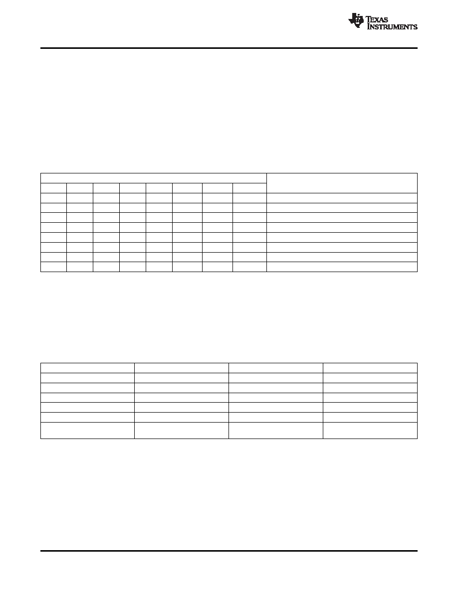
Table 5. CLKoutX_DIV: Clock Channel Divide Values
CLKoutX_DIV [ 7:0 ]
Total Divide Value
b7
b6
b5
b4
b3
b2
b1
b0
0
invalid
0
1
2
0
1
0
4
0
1
6
0
1
0
8
0
1
0
1
10
-
--
-
1
510
EN_CLKoutX: Clock Channel Output Enable
Each Clock Output Channel may be either enabled or disabled via the Clock Output Enable control bits. Each
output enable control bit is gated with the Global Output Enable input pin (GOE) and Global Output Enable bit
(EN_CLKout_Global). The GOE pin provides an internal pull-up so that if it is unterminated externally, the clock
output states are determined by the Clock Output Enable Register bits. All clock outputs can be set to the low
state simultaneously if the GOE pin is pulled low by an external signal. If EN_CLKout_Global is programmed to 0
all outputs are turned off. If both GOE and EN_CLKout_Global are low the clock outputs are turned off.
Table 6. EN_CLKoutX: Clock Channel Output Enable Control Bits
BIT NAME
BIT = 1
BIT = 0
DEFAULT
EN_CLKout0
ON
OFF
EN_CLKout1
ON
OFF
EN_CLKout2
ON
OFF
ON
EN_CLKout3
ON
OFF
EN_CLKout4
ON
OFF
EN_CLKout_Global
According to individual channel
All EN_CLKout X = OFF
-
settings
Note the default state of CLKout2 is ON after power on or RESET assertion. The nominal frequency is 62 MHz
(LMK040x1) or 81 MHz (LMK040x3). This is based on a channel divide value of 12 and default VCO_DIV value
of 2. If an active CLKout2 at power on is inappropriate for the user’s application, the following method can be
employed to shut off CLKout2 during system initialization:
When the device is powered on, holding the GOE pin LOW will disable all clock outputs. The device can be
programmed while the GOE is held LOW. The state of CLKout2 can be altered during device programming
according to the user’s specific application needs. After device configuration is complete, the GOE pin should
be set HIGH to enable the active clock channels.
32
Copyright 2008–2011, Texas Instruments Incorporated
相关PDF资料 |
PDF描述 |
|---|---|
| LMV393MUTAG | IC OP AMP DUAL GP LV LV 8-UDFN |
| LMX339HASD+T | IC COMPARATOR GP QUAD 14-SOIC |
| LT1011AIS8#TRPBF | IC VOLTAGE COMPARATOR 5V 8-SOIC |
| LT1016IS8#TRPBF | IC COMPARATOR 10NS HI-SPD 8-SOIC |
| LT1017IS8#TRPBF | IC COMPARATOR MICRPWR DUAL 8SOIC |
相关代理商/技术参数 |
参数描述 |
|---|---|
| LMK04010BISQX | 制造商:NSC 制造商全称:National Semiconductor 功能描述:Low-Noise Clock Jitter Cleaner with Cascaded PLLs |
| LMK04010BISQX/NOPB | 功能描述:时钟合成器/抖动清除器 RoHS:否 制造商:Skyworks Solutions, Inc. 输出端数量: 输出电平: 最大输出频率: 输入电平: 最大输入频率:6.1 GHz 电源电压-最大:3.3 V 电源电压-最小:2.7 V 封装 / 箱体:TSSOP-28 封装:Reel |
| LMK04011BISQ | 制造商:Texas Instruments 功能描述:Clock Conditioner 48-Pin LLP EP T/R |
| LMK04011BISQ/NOPB | 功能描述:时钟合成器/抖动清除器 RoHS:否 制造商:Skyworks Solutions, Inc. 输出端数量: 输出电平: 最大输出频率: 输入电平: 最大输入频率:6.1 GHz 电源电压-最大:3.3 V 电源电压-最小:2.7 V 封装 / 箱体:TSSOP-28 封装:Reel |
| LMK04011BISQE | 制造商:Texas Instruments 功能描述:Clock Conditioner 48-Pin LLP EP T/R 制造商:Texas Instruments 功能描述:PRECISION CLOCK CONDITIONER, 48LLP |
发布紧急采购,3分钟左右您将得到回复。