- 您现在的位置:买卖IC网 > PDF目录224146 > M470T6464EHS-CE6 DDR DRAM MODULE, ZMA200 PDF资料下载
参数资料
| 型号: | M470T6464EHS-CE6 |
| 元件分类: | DRAM |
| 英文描述: | DDR DRAM MODULE, ZMA200 |
| 封装: | ROHS COMPLIANT, SODIMM-200 |
| 文件页数: | 19/22页 |
| 文件大小: | 401K |
| 代理商: | M470T6464EHS-CE6 |
Rev. 1.0 August 2008
SODIMM
DDR2 SDRAM
6 of 22
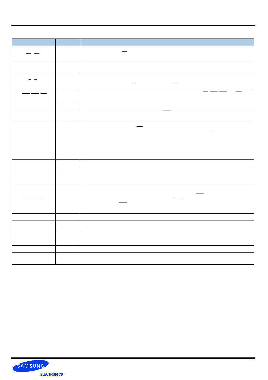
Symbol
Type
Description
CK0-CK1
Input
The system clock inputs. All address and command lines are sampled on the cross point of the rising edge
of CK and falling edge of CK . A Delay Locked Loop (DLL) circuit is driven from the clock input and output
timing for read operations is synchronized to the input clock.
CKE0-CKE1
Input
Activates the DDR2 SDRAM CK signal when high and deactivates the CK signal when low, By deactivating
the clocks, CKE low initiates the Power Down mode or the Self Refesh mode.
S0-S1
Input
Enables the associated DDR2 SDRAM command decoder when low and disables the command decoder
when high. When the command decoder is disabled, new commands are ignored but previous operations
continue. Rank 0 is selected by S0, Rank 1 is selected by S1. Ranks are also called “Physical banks”.
RAS, CAS, WE
Input
When sampled at the cross point of the rising edge of CK and falling edge of CK, CAS, RAS, and WE define
the operation to be executed by the SDRAM.
BA0~BA2
Input
Selects which DDR2 SDRAM internal bank is activated.
ODT0~ODT1
Input
Asserts on-die termination for DQ, DM, DQS, and DQS signals if enabled via the DDR2 SDRAM Extended
Mode Register Set (EMRS).
A0~A9,
A10/AP,
A11~A13
Input
During a Bank Activate command cycle, defines the row address when sampled at the cross point of the ris-
ing edge of CK and falling edge of CK. During a Read or Write command cycle, defines the column address
when sampled at the cross point of the rising edge of CK and falling edge of CK. In addition to the column
address, AP is used to invoke autoprecharge operation at the end of the burst read or write cycle. If AP is
high, autoprecharge is selected and BA0-BAn defines the bank to be precharged. If AP is low, autopre-
charge is disabled. During a Precharge command cycle, AP is used in conjunction with BA0-BAn to control
which bank(s) to precharge. If AP is high, all banks will be pecharged regardiess of the state of BA0-BAn
inputs. If AP is low, then BA0-BAn are used to define which bank to precharge.
DQ0~DQ63
In/Out
Data Input/Output pins.
DM0~DM7
Input
The data write masks, associated with one data byte. In Write mode, DM operates as a byte mask by allow-
ing input data to be written if it is low but blocks the write operation if it is high. In Read mode, DM lines have
no effect.
DQS0~DQS7
In/Out
The data strobes, associated with one data byte, sourced with data transfers. In Write mode, the data strobe
is sourced by the controller and is centered in the data window. In Read mode, the data strobe is sourced by
the DDR2 SDRAMs and is sent at the leading edge of the data window. DQS signals are complements, and
timing is relative to the crosspoint of respective DQS and DQS If the module is to be operated in single
ended strobe mode, all DQS signals must be tied on the system board to VSS and DDR2 SDRAM mode
registers programmed appropriately.
VDD,VDDSPD,VSS
Supply
Power supplies for core, I/O, Serial Presence Detect, and ground for the module.
SDA
In/Out
This is a bidirectional pin used to transfer data into or out of the SPD EEPROM. A resistor must be con-
nected to VDD to act as a pull up.
SCL
Input
This signal is used to clock data into and out of the SPD EEPROM. A resistor may be connected from SCL
to VDD to act as a pull up.
SA0~SA1
Input
Address pins used to select the Serial Presence Detect base address.
TEST
In/Out
The TEST pin is reserved for bus analysis tools and is not connected on normal memory modules(SO-
DIMMs).
6.0 Input/Output Function Description
相关PDF资料 |
PDF描述 |
|---|---|
| M470T6464EHS-LF7 | DDR DRAM MODULE, ZMA200 |
| M48T128V | 3.3V-5V 1 Mbit 128Kb x8 TIMEKEEPER SRAM |
| M48T12 | 16 Kbit 2Kb x8 TIMEKEEPER[ SRAM |
| M48T12-150PC1 | 16 Kbit 2Kb x8 TIMEKEEPER[ SRAM |
| M48T12-200PC1 | 16 Kbit 2Kb x8 TIMEKEEPER[ SRAM |
相关代理商/技术参数 |
参数描述 |
|---|---|
| M470T6464QZH3 | 制造商:SAMSUNG 制造商全称:Samsung semiconductor 功能描述:DDR2 SDRAM Memory |
| M470T6554BG0-CD5/CC | 制造商:SAMSUNG 制造商全称:Samsung semiconductor 功能描述:200pin Unbuffered SODIMM based on 512Mb B-die 64bit Non-ECC |
| M470T6554BG3-CD5/CC | 制造商:SAMSUNG 制造商全称:Samsung semiconductor 功能描述:200pin Unbuffered SODIMM based on 512Mb B-die 64bit Non-ECC |
| M470T6554BGZ0-CD5/CC | 制造商:SAMSUNG 制造商全称:Samsung semiconductor 功能描述:200pin Unbuffered SODIMM based on 512Mb B-die 64bit Non-ECC |
| M470T6554BGZ3-CD5/CC | 制造商:SAMSUNG 制造商全称:Samsung semiconductor 功能描述:200pin Unbuffered SODIMM based on 512Mb B-die 64bit Non-ECC |
发布紧急采购,3分钟左右您将得到回复。