- 您现在的位置:买卖IC网 > PDF目录5055 > MAX17080GTL+ (Maxim Integrated Products)IC CONTROLLER AMD SVI 40-TQFN PDF资料下载
参数资料
| 型号: | MAX17080GTL+ |
| 厂商: | Maxim Integrated Products |
| 文件页数: | 27/48页 |
| 文件大小: | 0K |
| 描述: | IC CONTROLLER AMD SVI 40-TQFN |
| 标准包装: | 60 |
| 应用: | 控制器,AMD SVI |
| 输入电压: | 2.7 V ~ 5.5 V |
| 输出数: | 3 |
| 输出电压: | 0.013 V ~ 1.55 V |
| 工作温度: | -40°C ~ 105°C |
| 安装类型: | 表面贴装 |
| 封装/外壳: | 40-WFQFN 裸露焊盘 |
| 供应商设备封装: | 40-TQFN-EP(5x5) |
| 包装: | 管件 |
第1页第2页第3页第4页第5页第6页第7页第8页第9页第10页第11页第12页第13页第14页第15页第16页第17页第18页第19页第20页第21页第22页第23页第24页第25页第26页当前第27页第28页第29页第30页第31页第32页第33页第34页第35页第36页第37页第38页第39页第40页第41页第42页第43页第44页第45页第46页第47页第48页
�� �
�
�AMD� 2-/3-Output� Mobile� Serial�
�VID� Controller�
�Nominal� Output-Voltage� Selection�
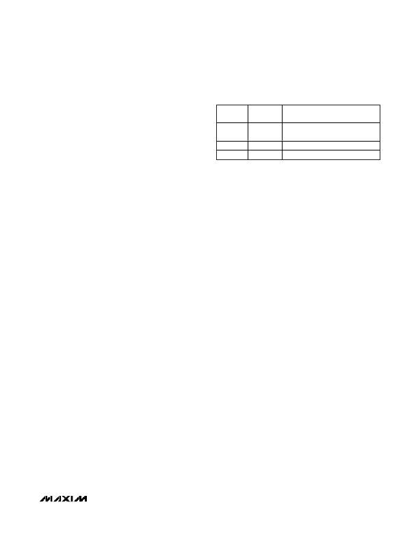
�Table� 3.� Boot� Voltage� Code� Table�
�Core� SMPS� Output� Voltage�
�The� nominal� no-load� output� voltage� (V� TARGET_� )� for�
�each� SMPS� is� defined� by� the� selected� voltage� refer-�
�ence� (VID� DAC)� plus� the� remote� ground-sense� adjust-�
�ment� (V� GNDS� )� and� the� offset� voltage� (V� OFFSET� )� as�
�defined� in� the� following� equation:�
�V� TARGET� =� V� FBDC� =� V� DAC� +� V� GNDS� +� V� OFFSET�
�SVC�
�0�
�0�
�1�
�1�
�SVD�
�0�
�1�
�0�
�1�
�BOOT� VOLTAGE�
�V� OUT� (V)�
�1.1�
�1.0�
�0.9�
�0.8�
�where� V� DAC� is� the� selected� VID� voltage� of� the� core�
�SMPS� DAC,� V� GNDS� is� the� ground-sense� correction� volt-�
�age� for� core� supplies,� and� V� OFFSET� is� the� +12.5mV� off-�
�set� enabled� by� the� OPTION� pin� when� the� PSI_L� is� set�
�high� for� core� supplies.�
�NB� SMPS� Output� Voltage�
�The� nominal� output� voltage� (V� TARGET� )� for� the� NB� is�
�defined� by� the� selected� voltage� reference� (VID� DAC)�
�plus� the� offset� voltage� (V� OFFSET_NB� )� as� defined� in� the�
�following� equation:�
�V� TARGET� 3� =� V� OUT� 3� =� V� DAC� +� V� OFFSET� _� NB�
�where� V� DAC� is� the� selected� VID� voltage� of� the� NB� DAC,�
�and� V� OFFSET_NB� is� +12.5mV� or� +6.25mV� as� set� by� the�
�ILIM3� pin� for� NB.�
�7-Bit� DAC�
�Inside� the� MAX17080� are� three� 7-bit� digital-to-analog�
�converters� (DACs).� Each� DAC� can� be� individually� pro-�
�grammed� to� different� voltage� levels� by� the� serial-inter-�
�face� bus.� The� DAC� sets� the� target� for� the� output� voltage�
�for� the� core� and� NB� SMPSs.� The� available� DAC� codes�
�and� resulting� output� voltages� are� compatible� with� the�
�AMD� SVI� (Table� 4)� specifications.�
�Boot� Voltage�
�On� startup,� the� MAX17080� slews� the� target� for� all� three�
�DACs� from� ground� to� the� boot� voltage� set� by� the� SVC�
�and� SVD� pin-voltage� levels.� While� the� output� is� still� below�
�regulation,� the� SVC� and� SVD� levels� can� be� changed,�
�and� the� MAX17080� sets� the� DACs� to� the� new� boot� volt-�
�age.� Once� the� programmed� boot� voltage� is� reached� and�
�PWRGD� goes� high,� the� MAX17080� stores� the� boot� VID.�
�Changes� in� the� SVC� and� SVD� settings� do� not� change� the�
�output� voltage� once� the� boot� VID� is� stored.� When�
�PGD_IN� goes� high,� the� MAX17080� exits� boot� mode,� and�
�the� three� DACs� can� be� independently� set� to� any� voltage�
�in� the� VID� table� by� the� serial� interface.�
�If� PGD_IN� goes� from� high� to� low� any� time� after� the� boot�
�VID� is� stored,� the� MAX17080� sets� all� three� DACs� back�
�to� the� voltage� of� the� stored� boot� VID.�
�Table� 3� is� the� boot� voltage� code� table.�
�Core� SMPS� Offset�
�A� +12.5mV� offset� can� be� added� to� both� core� SMPS�
�DAC� voltages� for� applications� that� include� DC� droop.�
�The� offset� is� applied� only� after� the� MAX17080� exits� boot�
�mode� (PGD_IN� going� from� low� to� high),� and� the�
�MAX17080� enters� the� serial-interface� mode.� The� offset�
�is� disabled� when� the� PSI_L� bit� is� set,� saving� more�
�power� when� the� load� is� light.�
�The� OPTION� pin� setting� enables� or� disables� the�
�+12.5mV� offset.� Connect� OPTION� to� OSC� (2V)� or� GND�
�to� enable� the� offset.� Keep� OPTION� connected� to� 3.3V�
�or� V� CC� to� disable� the� offset.� See� the� Offset� and�
�Address� Change� for� Core� SMPSs� (OPTION)� section.�
�NB� SMPS� Offset�
�The� NB� SMPS� output� has� a� -6.5mV/A� load-line.� An� off-�
�set� is� required� to� keep� the� output� within� regulation� over�
�the� full� load.� The� offset� is� set� by� the� ILIM3� pin� setting�
�(see� Table� 7).� Connect� ILIM3� to� OSC� (2V)� or� GND� to�
�set� a� +6.25mV� offset.� Pull� the� ILIM3� pin� up� to� 3.3V� or�
�V� CC� to� set� +12.5mV� offset.� See� the� Offset� and� Current-�
�Limit� Setting� for� NB� SMPS� (ILIM3)� section.�
�Output-Voltage� Transition� Timing�
�SMPS� Output-Voltage� Transition�
�The� MAX17080� performs� positive� voltage� transitions� in�
�a� controlled� manner,� automatically� minimizing� input�
�surge� currents.� This� feature� allows� the� circuit� designer�
�to� achieve� nearly� ideal� transitions,� guaranteeing� just-in-�
�time� arrival� at� the� new� output-voltage� level� with� the� low-�
�est� possible� peak� currents� for� a� given� output�
�capacitance.� The� slew� rate� (set� by� resistor� R� TIME� )� must�
�be� set� fast� enough� to� ensure� that� the� transition� is� com-�
�pleted� within� the� maximum� allotted� time� for� proper� CPU�
�operation.� R� TIME� is� between� 35.7k� ?� and� 357k� ?� for� cor-�
�responding� slew� rates� between� 25mV/μs� to� 2.5mV/μs,�
�respectively,� for� the� SMPSs.�
�At� the� beginning� of� an� output-voltage� transition,� the�
�MAX17080� blanks� both� PWRGD� comparator� thresholds,�
�preventing� the� PWRGD� open-drain� output� from� chang-�
�ing� states� during� the� transition.� At� the� end� of� an� upward�
�VID� transition,� the� controller� enables� both� PWRGD�
�thresholds� approximately� 20μs� after� the� slew-rate�
�______________________________________________________________________________________�
�27�
�相关PDF资料 |
PDF描述 |
|---|---|
| GBA49DRMS | CONN EDGECARD 98POS .125 SQ WW |
| X5649S14I-2.7A | IC SUPERVISOR CPU 64K EE 14-SOIC |
| X5649S14I-2.7 | IC SUPERVISOR CPU 64K EE 14-SOIC |
| P1330R-333K | INDUCTOR POWER 33.0UH SMD |
| P1330-333K | INDUCTOR POWER 33.0UH SMD |
相关代理商/技术参数 |
参数描述 |
|---|---|
| MAX17080GTL+ | 功能描述:开关变换器、稳压器与控制器 Integrated Circuits (ICs) Voltage Regulators - Special Purpose - IC CONTROLLER AMD SVI 40-TQFN RoHS:否 制造商:Texas Instruments 输出电压:1.2 V to 10 V 输出电流:300 mA 输出功率: 输入电压:3 V to 17 V 开关频率:1 MHz 工作温度范围: 安装风格:SMD/SMT 封装 / 箱体:WSON-8 封装:Reel |
| MAX17080GTL+T | 功能描述:开关变换器、稳压器与控制器 Integrated Circuits (ICs) Voltage Regulators - Special Purpose - IC CONTROLLER AMD SVI 40-TQFN RoHS:否 制造商:Texas Instruments 输出电压:1.2 V to 10 V 输出电流:300 mA 输出功率: 输入电压:3 V to 17 V 开关频率:1 MHz 工作温度范围: 安装风格:SMD/SMT 封装 / 箱体:WSON-8 封装:Reel |
| MAX17081EVKIT+ | 功能描述:电源管理IC开发工具 RoHS:否 制造商:Maxim Integrated 产品:Evaluation Kits 类型:Battery Management 工具用于评估:MAX17710GB 输入电压: 输出电压:1.8 V |
| MAX17081EWV+ | 功能描述:电池管理 RoHS:否 制造商:Texas Instruments 电池类型:Li-Ion 输出电压:5 V 输出电流:4.5 A 工作电源电压:3.9 V to 17 V 最大工作温度:+ 85 C 最小工作温度:- 40 C 封装 / 箱体:VQFN-24 封装:Reel |
| MAX17081EWV+T | 功能描述:电池管理 RoHS:否 制造商:Texas Instruments 电池类型:Li-Ion 输出电压:5 V 输出电流:4.5 A 工作电源电压:3.9 V to 17 V 最大工作温度:+ 85 C 最小工作温度:- 40 C 封装 / 箱体:VQFN-24 封装:Reel |
发布紧急采购,3分钟左右您将得到回复。