- 您现在的位置:买卖IC网 > PDF目录13110 > MAX8550AETI+ (Maxim Integrated Products)IC PWR SUP DDR INTEG 28TQFN PDF资料下载
参数资料
| 型号: | MAX8550AETI+ |
| 厂商: | Maxim Integrated Products |
| 文件页数: | 17/29页 |
| 文件大小: | 0K |
| 描述: | IC PWR SUP DDR INTEG 28TQFN |
| 产品培训模块: | Lead (SnPb) Finish for COTS Obsolescence Mitigation Program |
| 标准包装: | 60 |
| 应用: | 控制器,DDR |
| 输入电压: | 2 V ~ 28 V |
| 输出数: | 2 |
| 输出电压: | 1.8V,2.5V,0.7 V ~ 5.5 V |
| 工作温度: | -40°C ~ 85°C |
| 安装类型: | 表面贴装 |
| 封装/外壳: | 28-WFQFN 裸露焊盘 |
| 供应商设备封装: | 28-TQFN-EP(5x5) |
| 包装: | 管件 |
第1页第2页第3页第4页第5页第6页第7页第8页第9页第10页第11页第12页第13页第14页第15页第16页当前第17页第18页第19页第20页第21页第22页第23页第24页第25页第26页第27页第28页第29页
�� �
�
�Integrated� DDR� Power-Supply� Solution� for�
�Desktops,� Notebooks,� and� Graphic� Cards�
�Overvoltage� Protection� (OVP)�
�When� the� output� voltage� rises� above� 116%� of� the� nomi-�
�nal� regulation� voltage� and� OVP� is� enabled� (OVP/UVP� =�
�AV� DD� or� open),� the� OVP� circuit� sets� the� fault� latch,�
�shuts� down� the� PWM� controller,� and� immediately� pulls�
�DH� low� and� forces� DL� high.� This� turns� on� the� synchro-�
�nous-rectifier� MOSFET� (Q2� in� the� Typical� Applications�
�Circuit� of� Figure� 8)� with� a� 100%� duty� cycle,� rapidly� dis-�
�charging� the� output� capacitor� and� clamping� the� output�
�to� ground.� Note� that� immediately� latching� DL� high� can�
�cause� the� output� voltage� to� go� slightly� negative� due� to�
�energy� stored� in� the� output� LC� circuit� at� the� instant� the�
�OVP� occurs.� If� the� load� cannot� tolerate� a� negative� volt-�
�age,� place� a� power� Schottky� diode� across� the� output� to�
�act� as� a� reverse-polarity� clamp.� Toggle� SHDN� or� cycle�
�AV� DD� below� 1V� to� clear� the� fault� latch� and� restart� the�
�controller.� OVP� is� disabled� when� OVP/UVP� is� connect-�
�ed� to� REF� or� GND� (see� Table� 3).� OVP� only� applies� to�
�the� buck� output.� The� VTT� and� VTTR� outputs� do� not�
�have� overvoltage� protection.�
�Undervoltage� Protection� (UVP)�
�When� the� output� voltage� drops� below� 70%� of� its� regula-�
�tion� voltage� while� UVP� is� enabled,� the� controller� sets�
�the� fault� latch� and� begins� the� discharge� mode� (see� the�
�Shutdown� and� Output� Discharge� section).� When� the�
�output� voltage� drops� to� 0.1V,� the� synchronous� rectifier�
�(Q2� in� the� Typical� Applications� Circuit� )� turns� on� and�
�clamps� the� buck� output� to� GND.� UVP� is� ignored� for� at�
�least� 10ms� (min)� after� startup� or� after� a� rising� edge� on�
�SHDN� .� Toggle� SHDN� or� cycle� AV� DD� power� below� 1V� to�
�clear� the� fault� latch� and� restart� the� controller.� UVP� is�
�disabled� when� OVP/UVP� is� left� open� or� connected� to�
�GND� (see� Table� 3).� UVP� only� applies� to� the� buck� out-�
�put.� The� VTT� and� VTTR� outputs� do� not� have� undervolt-�
�age� protection.�
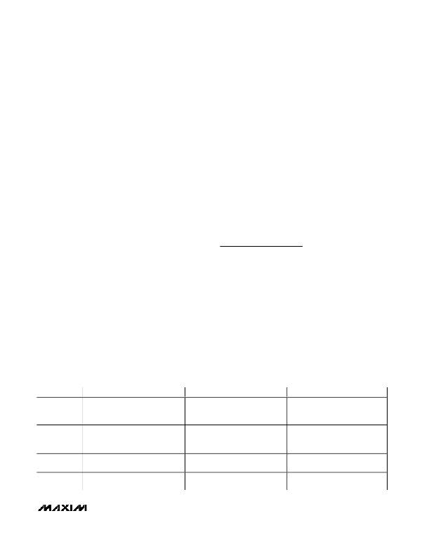
�Table� 3.� OVP/UVP� Fault� Protection�
�Thermal� Fault� Protection�
�The� MAX8550A� features� two� thermal-fault-protection�
�circuits.� One� monitors� the� buck-regulator� portion� of� the�
�IC� and� the� other� monitors� the� linear� regulator� (VTT)� and�
�the� reference� buffer� output� (VTTR).� When� the� junction�
�temperature� of� the� buck-regulator� portion� of� the�
�MAX8550A� rises� above� +160°C,� a� thermal� sensor� acti-�
�vates� the� fault� latch,� pulls� POK1� low,� and� shuts� down�
�the� buck-controller� output� using� discharge� mode�
�regardless� of� the� OVP/UVP� setting.� Toggle� SHDN� or�
�cycle� AV� DD� below� 1V� to� reactivate� the� controller� after�
�the� junction� temperature� cools� by� 15°C.� If� the� VTT� and�
�VTTR� regulator� portion� of� the� IC� has� its� die� temperature�
�rise� above� +160� °� C,� then� VTT� and� VTTR� shut� off,� go�
�high� impedance,� and� restart� after� the� die� portion� of� the�
�IC� cools� by� 15� °� C.� Both� thermal� faults� are� independent.�
�For� example,� if� the� VTT� output� is� overloaded� to� the�
�point� that� it� triggers� its� thermal� fault,� the� buck� regulator�
�continues� to� function.�
�Design� Procedure�
�Firmly� establish� the� input� voltage� range� (V� IN� )� and� maxi-�
�mum� load� current� (I� LOAD� )� in� the� buck� regulator� before�
�choosing� a� switching� frequency� and� inductor� operating�
�point� (ripple� current� ratio� or� LIR).� The� primary� design�
�trade-off� lies� in� choosing� a� good� switching� frequency�
�and� inductor� operating� point,� and� the� following� four� fac-�
�tors� dictate� the� rest� of� the� design:�
�?� Input� Voltage� Range.� The� maximum� value� (V� IN(MAX)� )�
�must� accommodate� the� worst-case� voltage.� The� mini-�
�mum� value� (V� IN(MIN)� )� must� account� for� the� lowest�
�voltage� after� drops� due� to� connectors� and� fuses.� If�
�there� is� a� choice,� lower� input� voltages� result� in� better�
�efficiency.�
�OVP/UVP�
�DISCHARGE�
�UVP� PROTECTION�
�OVP� PROTECTION�
�Yes.�
�AV� DD�
�DL� forced� high� when� SHDN� is� low�
�Enabled�
�Enabled�
�and� OUT� <� 0.1V.�
�Yes.�
�OPEN�
�DL� forced� high� when� SHDN� is� low�
�Disabled�
�Enabled�
�and� OUT� <� 0.1V.�
�REF�
�GND�
�No.�
�DL� forced� low� when� SHDN� is� low.�
�No.�
�DL� forced� low� when� SHDN� is� low.�
�Enabled�
�Disabled�
�Disabled�
�Disabled�
�______________________________________________________________________________________�
�17�
�相关PDF资料 |
PDF描述 |
|---|---|
| MAX8632ETI+ | IC PWR SUPPLY DDR 28-TQFN |
| VE-J1B-CZ-B1 | CONVERTER MOD DC/DC 95V 25W |
| ASC15DRAN | CONN EDGECARD 30POS .100 R/A DIP |
| MAX17582GTM+ | IC PWM CTRLR STP-DN DL 48TQFN |
| RMM18DTAS | CONN EDGECARD 36POS R/A .156 SLD |
相关代理商/技术参数 |
参数描述 |
|---|---|
| MAX8550AETI+ | 功能描述:电压模式 PWM 控制器 Integrated DDR Power Supply Solution RoHS:否 制造商:Texas Instruments 输出端数量:1 拓扑结构:Buck 输出电压:34 V 输出电流: 开关频率: 工作电源电压:4.5 V to 5.5 V 电源电流:600 uA 最大工作温度:+ 125 C 最小工作温度:- 40 C 封装 / 箱体:WSON-8 封装:Reel |
| MAX8550AETI+T | 功能描述:电压模式 PWM 控制器 Integrated DDR Power Supply Solution RoHS:否 制造商:Texas Instruments 输出端数量:1 拓扑结构:Buck 输出电压:34 V 输出电流: 开关频率: 工作电源电压:4.5 V to 5.5 V 电源电流:600 uA 最大工作温度:+ 125 C 最小工作温度:- 40 C 封装 / 箱体:WSON-8 封装:Reel |
| MAX8550AETI-T | 功能描述:PMIC 解决方案 RoHS:否 制造商:Texas Instruments 安装风格:SMD/SMT 封装 / 箱体:QFN-24 封装:Reel |
| MAX8550ETI | 功能描述:PMIC 解决方案 RoHS:否 制造商:Texas Instruments 安装风格:SMD/SMT 封装 / 箱体:QFN-24 封装:Reel |
| MAX8550ETI+ | 功能描述:电压模式 PWM 控制器 Integrated DDR Power Supply Solution RoHS:否 制造商:Texas Instruments 输出端数量:1 拓扑结构:Buck 输出电压:34 V 输出电流: 开关频率: 工作电源电压:4.5 V to 5.5 V 电源电流:600 uA 最大工作温度:+ 125 C 最小工作温度:- 40 C 封装 / 箱体:WSON-8 封装:Reel |
发布紧急采购,3分钟左右您将得到回复。