- 您现在的位置:买卖IC网 > PDF目录13110 > MAX8550AETI+ (Maxim Integrated Products)IC PWR SUP DDR INTEG 28TQFN PDF资料下载
参数资料
| 型号: | MAX8550AETI+ |
| 厂商: | Maxim Integrated Products |
| 文件页数: | 18/29页 |
| 文件大小: | 0K |
| 描述: | IC PWR SUP DDR INTEG 28TQFN |
| 产品培训模块: | Lead (SnPb) Finish for COTS Obsolescence Mitigation Program |
| 标准包装: | 60 |
| 应用: | 控制器,DDR |
| 输入电压: | 2 V ~ 28 V |
| 输出数: | 2 |
| 输出电压: | 1.8V,2.5V,0.7 V ~ 5.5 V |
| 工作温度: | -40°C ~ 85°C |
| 安装类型: | 表面贴装 |
| 封装/外壳: | 28-WFQFN 裸露焊盘 |
| 供应商设备封装: | 28-TQFN-EP(5x5) |
| 包装: | 管件 |
第1页第2页第3页第4页第5页第6页第7页第8页第9页第10页第11页第12页第13页第14页第15页第16页第17页当前第18页第19页第20页第21页第22页第23页第24页第25页第26页第27页第28页第29页
�� �
�
�Integrated� DDR� Power-Supply� Solution� for�
�Desktops,� Notebooks,� and� Graphic� Cards�
�?� Maximum� Load� Current.� There� are� two� values� to� con-�
�sider.� The� peak� load� current� (I� PEAK� )� determines� the�
�instantaneous� component� stresses� and� filtering�
�requirements� and� thus� drives� output� capacitor� selec-�
�tion,� inductor� saturation� rating,� and� the� design� of� the�
�current-limit� circuit.� The� continuous� load� current�
�(I� LOAD� )� determines� the� thermal� stresses� and� thus�
�drives� the� selection� of� input� capacitors,� MOSFETs,�
�and� other� critical� heat-contributing� components.�
�?� Switching� Frequency.� This� choice� determines� the�
�basic� trade-off� between� size� and� efficiency.� The� opti-�
�mal� frequency� is� largely� a� function� of� maximum� input�
�voltage,� due� to� MOSFET� switching� losses� proportion-�
�al� to� frequency� and� V� IN� 2� .� The� optimum� frequency� is�
�also� a� moving� target� due� to� rapid� improvements� in�
�MOSFET� technology� that� are� making� higher� frequen-�
�cies� more� practical.�
�?� Inductor� Operating� Point.� This� choice� provides� trade-�
�offs:� size� vs.� efficiency� and� transient� response� vs.� out-�
�put� ripple.� Low� inductor� values� provide� better�
�where� V� FB� is� 0.7V,� R� C� and� R� D� are� shown� in� Figure� 6,�
�and� V� RIPPLE� is:�
�V� RIPPLE� =� LIR� � I� LOAD� (� MAX� )� � R� ESR�
�Setting� the� VTT� and� VTTR� Voltages� (LDO)�
�The� termination� power-supply� output� (VTT)� can� be� set� by�
�two� different� methods.� First,� the� VTT� output� can� be� con-�
�nected� directly� to� the� VTTS� input� to� force� VTT� to� regulate�
�to� V� REFIN� /� 2.� Secondly,� VTT� can� be� forced� to� regulate�
�higher� than� V� REFIN� /� 2� by� connecting� a� resistive� divider�
�from� VTT� to� VTTS.� The� maximum� value� for� VTT� is� V� VTTI� -�
�V� DROPOUT� where� V� DROPOUT� =� I� VTT� ×� 0.3� Ω� (max)� at� T� A�
�=� +85°C.�
�The� termination� reference� voltage� (VTTR)� tracks� 1/2�
�V� REFIN� .�
�Inductor� Selection� (Buck)�
�The� switching� frequency� and� inductor� operating� point�
�determine� the� inductor� value� as� follows:�
�V� OUT� (� V� IN� OUT� )�
�transient� response� and� smaller� physical� size� but� also�
�result� in� lower� efficiency� and� higher� output� ripple� due�
�to� increased� ripple� currents.� The� minimum� practical�
�inductor� value� is� one� that� causes� the� circuit� to� operate�
�L� =�
�-� V�
�V� IN� � f� SW� � I� LOAD� (� MAX� )� � LIR�
�at� the� edge� of� critical� conduction� (where� the� inductor�
�current� just� touches� zero� with� every� cycle� at� maximum�
�For� example:� I� LOAD(MAX)� =� 12A,� V� IN� =� 12V,� V� OUT� =�
�2.5V,� f� SW� =� 600kHz,� 30%� ripple� current� or� LIR� =� 0.3:�
�load).� Inductor� values� lower� than� this� grant� no� further�
�size-reduction� benefit.� The� optimum� operating� point� is�
�usually� found� between� 20%� and� 50%� ripple� current.�
�When� pulse� skipping� (� SKIP� =� low� at� light� loads),� the�
�L� =�
�2� .� 5� V� (� 12� V� -� 2.5V)�
�12� V� � 600� kHz� � 12� A� � 0� .� 3�
�≈� 1� μ� H�
�inductor� value� also� determines� the� load-current� value�
�at� which� PFM/PWM� switchover� occurs.�
�Setting� the� Output� Voltage� (Buck)�
�Preset� Output� Voltages�
�The� MAX8550A� dual-mode� operation� allows� the� selec-�
�tion� of� common� voltages� without� requiring� external�
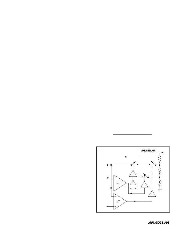
�components� (Figure� 5).� Connect� FB� to� GND� for� a� fixed�
�FB�
�TO�
�ERROR�
�AMPLIFIER�
�MAX8550A�
�OUT�
�1.8V�
�(FIXED)�
�2.5V� output,� to� AV� DD� for� a� fixed� 1.8V� output,� or� connect�
�FB� directly� to� OUT� for� a� fixed� 0.7V� output.�
�Setting� the� Buck� Regulator� Output� (V� OUT� )� with� a�
�Resistive� Voltage-Divider� at� FB�
�The� buck-regulator� output� voltage� can� be� adjusted� from�
�0.7V� to� 5.5V� using� a� resistive� voltage-divider� (Figure� 6).�
�The� MAX8550A� regulates� FB� to� a� fixed� reference� volt-�
�age� (0.7V).� The� adjusted� output� voltage� is:�
�REF� (2.0V)�
�2.5V�
�(FIXED)�
�V� OUT� FB� ?� 1� +�
�=� V�
�?�
�?�
�R� C� ?�
�R� D� ?� ?�
�+�
�V� RIPPLE�
�2�
�0.1V�
�Figure� 5.� Dual-Mode� Feedback� Decoder�
�18�
�______________________________________________________________________________________�
�相关PDF资料 |
PDF描述 |
|---|---|
| MAX8632ETI+ | IC PWR SUPPLY DDR 28-TQFN |
| VE-J1B-CZ-B1 | CONVERTER MOD DC/DC 95V 25W |
| ASC15DRAN | CONN EDGECARD 30POS .100 R/A DIP |
| MAX17582GTM+ | IC PWM CTRLR STP-DN DL 48TQFN |
| RMM18DTAS | CONN EDGECARD 36POS R/A .156 SLD |
相关代理商/技术参数 |
参数描述 |
|---|---|
| MAX8550AETI+ | 功能描述:电压模式 PWM 控制器 Integrated DDR Power Supply Solution RoHS:否 制造商:Texas Instruments 输出端数量:1 拓扑结构:Buck 输出电压:34 V 输出电流: 开关频率: 工作电源电压:4.5 V to 5.5 V 电源电流:600 uA 最大工作温度:+ 125 C 最小工作温度:- 40 C 封装 / 箱体:WSON-8 封装:Reel |
| MAX8550AETI+T | 功能描述:电压模式 PWM 控制器 Integrated DDR Power Supply Solution RoHS:否 制造商:Texas Instruments 输出端数量:1 拓扑结构:Buck 输出电压:34 V 输出电流: 开关频率: 工作电源电压:4.5 V to 5.5 V 电源电流:600 uA 最大工作温度:+ 125 C 最小工作温度:- 40 C 封装 / 箱体:WSON-8 封装:Reel |
| MAX8550AETI-T | 功能描述:PMIC 解决方案 RoHS:否 制造商:Texas Instruments 安装风格:SMD/SMT 封装 / 箱体:QFN-24 封装:Reel |
| MAX8550ETI | 功能描述:PMIC 解决方案 RoHS:否 制造商:Texas Instruments 安装风格:SMD/SMT 封装 / 箱体:QFN-24 封装:Reel |
| MAX8550ETI+ | 功能描述:电压模式 PWM 控制器 Integrated DDR Power Supply Solution RoHS:否 制造商:Texas Instruments 输出端数量:1 拓扑结构:Buck 输出电压:34 V 输出电流: 开关频率: 工作电源电压:4.5 V to 5.5 V 电源电流:600 uA 最大工作温度:+ 125 C 最小工作温度:- 40 C 封装 / 箱体:WSON-8 封装:Reel |
发布紧急采购,3分钟左右您将得到回复。