- 您现在的位置:买卖IC网 > PDF目录80563 > MC68HC05C5CP (MOTOROLA INC) 8-BIT, MROM, 2.1 MHz, MICROCONTROLLER, PDIP40 PDF资料下载
参数资料
| 型号: | MC68HC05C5CP |
| 厂商: | MOTOROLA INC |
| 元件分类: | 微控制器/微处理器 |
| 英文描述: | 8-BIT, MROM, 2.1 MHz, MICROCONTROLLER, PDIP40 |
| 封装: | DIP-40 |
| 文件页数: | 40/58页 |
| 文件大小: | 166K |
| 代理商: | MC68HC05C5CP |
第1页第2页第3页第4页第5页第6页第7页第8页第9页第10页第11页第12页第13页第14页第15页第16页第17页第18页第19页第20页第21页第22页第23页第24页第25页第26页第27页第28页第29页第30页第31页第32页第33页第34页第35页第36页第37页第38页第39页当前第40页第41页第42页第43页第44页第45页第46页第47页第48页第49页第50页第51页第52页第53页第54页第55页第56页第57页第58页
Page 39
Section 7: Simple Input/Output Port
MOTOROLA
MC68HC05C5 Specification Rev. 1.2
SECTION 7
SIMPLE SERIAL INPUT/OUTPUT PORT
This device includes a simple synchronous Serial I/O Port (SIOP). The SIOP is a three-
wire master/slave system including Serial Clock (SCK), Serial Data Input (SDI), and Serial
Data Output (SDO). A mask programmable option determines whether the SIOP is MSB
or LSB first.
7.1
SIGNAL FORMAT
7.1.1
SCK
The state of SCK between transmissions must be logic ’1’ for CPOL set and logic ’0’ for
CPOL clear. The first transition of SCK signals the beginning of a transmission. At this
time, the first bit of received data is accepted at the SDI pin and the first bit of transmitted
data is presented at the SDO pin. Data is captured at the SDI pin on the rising edge of
SCK. Subsequent falling edges shift the data and accept or present the next bit. The
transmission is ended upon the eighth rising edge of SCK. The maximum frequency of
SCK in slave mode is equal to E (bus clock) divided by 4. That is for a 4 MHz oscillator
input E becomes 2 MHz and the maximum SCK frequency is 500 KHz. There is no
minimum SCK frequency.
In master mode, the format is identical except that the SCK pin is an output and the shift
clock now originates internally. The master mode transmission frequency is fixed at E/4.
7.1.2
SDO
A mask programmable option will be included to allow data to be transmitted in either MSB
first format or LSB first format. In either case, the state of the SDO pin will always reflect
the value of the first bit received on the previous transmission if there was one. Upon
enabling the SIOP, SDO will always be driven to a logic one by the SIOP subsystem.
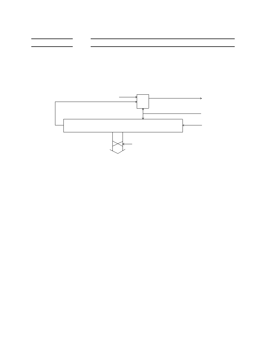
Figure 7-1: SIOP Block Diagram
8-BIT SHIFT REGISTER
D
Q
R
C
RESET
SDO
SCK
SDI
MSB/LSB MASK OPTION
DATA BUS
相关PDF资料 |
PDF描述 |
|---|---|
| MB89475PFV | 8-BIT, 12.5 MHz, MICROCONTROLLER, PQFP48 |
| MAH28151FXXXX | 1 CHANNEL(S), 64K bps, SERIAL COMM CONTROLLER, CQFP68 |
| MPC8245LZU300D | 32-BIT, 300 MHz, RISC PROCESSOR, PBGA352 |
| MPC8250AZUMHBB | 32-BIT, 266 MHz, RISC PROCESSOR, PBGA480 |
| MPC859DSLZP66 | 32-BIT, 66 MHz, RISC PROCESSOR, PBGA357 |
相关代理商/技术参数 |
参数描述 |
|---|---|
| MC68HC05C8 | 制造商:MOTOROLA 制造商全称:Motorola, Inc 功能描述:PROGRAMMING REFRERENCE GUIDE |
| MC68HC05C8A | 制造商:MOTOROLA 制造商全称:Motorola, Inc 功能描述:Microcontrollers |
| MC68HC05C8ACFN | 制造商:Motorola Inc 功能描述:MicroController, 8-Bit, 44 Pin, Plastic, PLCC |
| MC68HC05C9 | 制造商:FREESCALE 制造商全称:Freescale Semiconductor, Inc 功能描述:TECHNICAL DATA |
| MC68HC05C9A | 制造商:FREESCALE 制造商全称:Freescale Semiconductor, Inc 功能描述:Microcontrollers |
发布紧急采购,3分钟左右您将得到回复。