- 您现在的位置:买卖IC网 > PDF目录98015 > MJE13009BV (ON SEMICONDUCTOR) 12 A, 400 V, NPN, Si, POWER TRANSISTOR PDF资料下载
参数资料
| 型号: | MJE13009BV |
| 厂商: | ON SEMICONDUCTOR |
| 元件分类: | 功率晶体管 |
| 英文描述: | 12 A, 400 V, NPN, Si, POWER TRANSISTOR |
| 封装: | PLASTIC, TO-220AB, 3 PIN |
| 文件页数: | 45/65页 |
| 文件大小: | 517K |
| 代理商: | MJE13009BV |
第1页第2页第3页第4页第5页第6页第7页第8页第9页第10页第11页第12页第13页第14页第15页第16页第17页第18页第19页第20页第21页第22页第23页第24页第25页第26页第27页第28页第29页第30页第31页第32页第33页第34页第35页第36页第37页第38页第39页第40页第41页第42页第43页第44页当前第45页第46页第47页第48页第49页第50页第51页第52页第53页第54页第55页第56页第57页第58页第59页第60页第61页第62页第63页第64页第65页
MJE13009
3–680
Motorola Bipolar Power Transistor Device Data
t1
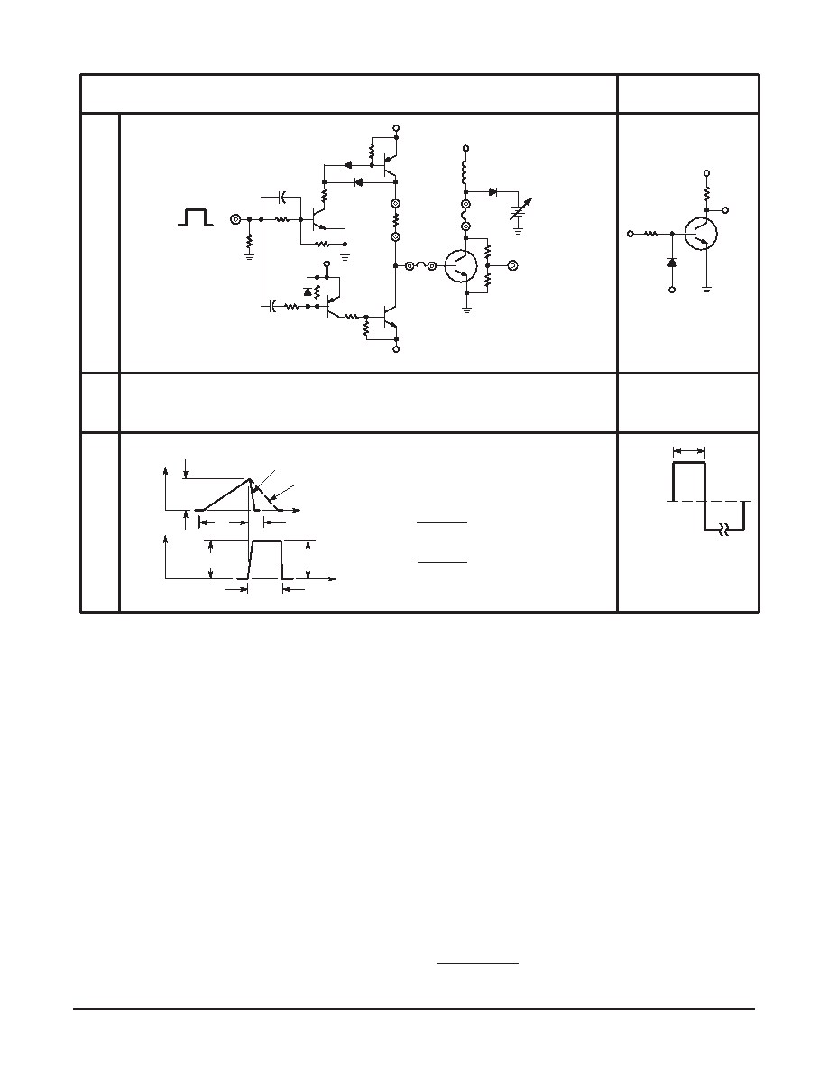
REVERSE BIAS SAFE OPERATING AREA AND INDUCTIVE SWITCHING
RESISTIVE
SWITCHING
OUTPUT WAVEFORMS
TEST
CIRCUITS
CIRCUIT
V
ALUES
TEST
W
A
VEFORMS
NOTE
PW and VCC Adjusted for Desired IC
RB Adjusted for Desired IB1
5 V
PW
DUTY CYCLE
≤ 10%
tr, tf ≤ 10 ns
68
1 k
0.001
F
0.02
F
1N4933
270
+5 V
1 k
2N2905
47
1/2 W
100
–VBE(off)
MJE200
D.U.T.
IB
RB
1N4933
33
2N2222
1 k
MJE210
VCC
+5 V
L
IC
MR826*
Vclamp
*SELECTED FOR
≥ 1 kV
VCE
5.1 k
51
+125 V
RC
SCOPE
– 4.0 V
D1
RB
TUT
t1 ADJUSTED TO
OBTAIN IC
t1 ≈
Lcoil (ICM)
VCC
t2 ≈
Lcoil (ICM)
Vclamp
+10 V
25
s
0
–8 V
Coil Data:
Ferroxcube Core #6656
Full Bobbin (~16 Turns) #16
GAP for 200
H/20 A
Lcoil = 200 H
VCC = 20 V
Vclamp = 300 Vdc
VCC = 125 V
RC = 15
D1 = 1N5820 or Equiv.
RB =
Test Equipment
Scope–Tektronics
475 or Equivalent
tr, tf < 10 ns
Duty Cycle = 1.0%
RB and RC adjusted
for desired IB and IC
IC
VCE
TIME
ICM
VCEM
t2
t
tf
tf CLAMPED
tf UNCLAMPED ≈ t2
Vclamp
Table 1. Test Conditions for Dynamic Performance
APPLICATIONS INFORMATION FOR SWITCHMODE SPECIFICATIONS
INTRODUCTION
The primary considerations when selecting a power tran-
sistor for SWITCHMODE applications are voltage and cur-
rent ratings, switching speed, and energy handling capability.
In this section, these specifications will be discussed and re-
lated to the circuit examples illustrated in Table 2.(1)
VOLTAGE REQUIREMENTS
Both blocking voltage and sustaining voltage are important
in SWITCHMODE applications.
Circuits B and C in Table 2 illustrate applications that re-
quire high blocking voltage capability. In both circuits the
switching transistor is subjected to voltages substantially
higher than VCC after the device is completely off (see load
line diagrams at IC = Ileakage ≈ 0 in Table 2). The blocking ca-
pability at this point depends on the base to emitter condi-
tions and the device junction temperature. Since the highest
device capability occurs when the base to emitter junction is
reverse biased (VCEV), this is the recommended and speci-
fied use condition. Maximum ICEV at rated VCEV is specified
at a relatively low reverse bias (1.5 Volts) both at 25
°C and
100
_C. Increasing the reverse bias will give some improve-
ment in device blocking capability.
The sustaining or active region voltage requirements in
switching applications occur during turn–on and turn–off. If
the load contains a significant capacitive component, high
current and voltage can exist simultaneously during turn–on
and the pulsed forward bias SOA curves (Figure 1) are the
proper design limits.
For inductive loads, high voltage and current must be sus-
tained simultaneously during turn–off, in most cases, with the
base to emitter junction reverse biased. Under these condi-
tions the collector voltage must be held to a safe level at or
below a specific value of collector current. This can be ac-
complished by several means such as active clamping, RC
snubbing, load line shaping, etc. The safe level for these de-
vices is specified as a Reverse Bias Safe Operating Area
(Figure 2) which represents voltage–current conditions that
can be sustained during reverse biased turn–off. This rating
is verified under clamped conditions so that the device is
never subjected to an avalanche mode.
(1) For detailed information on specific switching applications, see
Motorola Application Notes AN–719, AN–767.
相关PDF资料 |
PDF描述 |
|---|---|
| MJE13009BG | 12 A, 400 V, NPN, Si, POWER TRANSISTOR |
| MJE1320DW | 2 A, 900 V, NPN, Si, POWER TRANSISTOR |
| MJE1320BV | 2 A, 900 V, NPN, Si, POWER TRANSISTOR |
| MJE1320BA | 2 A, 900 V, NPN, Si, POWER TRANSISTOR |
| MJE1320AN | 2 A, 900 V, NPN, Si, POWER TRANSISTOR |
相关代理商/技术参数 |
参数描述 |
|---|---|
| MJE13009D | 制造商:UTC-IC 制造商全称:UTC-IC 功能描述:HIGH VOLTAGE FAST-SWITCHING NPN POWER TRANSISTOR |
| MJE13009DG-TA3-T | 制造商:UTC-IC 制造商全称:UTC-IC 功能描述:HIGH VOLTAGE FAST-SWITCHING NPN POWER TRANSISTOR |
| MJE13009DL-TA3-T | 制造商:UTC-IC 制造商全称:UTC-IC 功能描述:HIGH VOLTAGE FAST-SWITCHING NPN POWER TRANSISTOR |
| MJE13009F | 制造商:KEC 制造商全称:KEC(Korea Electronics) 功能描述:TRIPLE DIFFUSED NPN TRANSISTOR |
| MJE13009G | 功能描述:两极晶体管 - BJT 12A 400V 100W NPN RoHS:否 制造商:STMicroelectronics 配置: 晶体管极性:PNP 集电极—基极电压 VCBO: 集电极—发射极最大电压 VCEO:- 40 V 发射极 - 基极电压 VEBO:- 6 V 集电极—射极饱和电压: 最大直流电集电极电流: 增益带宽产品fT: 直流集电极/Base Gain hfe Min:100 A 最大工作温度: 安装风格:SMD/SMT 封装 / 箱体:PowerFLAT 2 x 2 |
发布紧急采购,3分钟左右您将得到回复。