- 您现在的位置:买卖IC网 > PDF目录98015 > MJE13009BV (ON SEMICONDUCTOR) 12 A, 400 V, NPN, Si, POWER TRANSISTOR PDF资料下载
参数资料
| 型号: | MJE13009BV |
| 厂商: | ON SEMICONDUCTOR |
| 元件分类: | 功率晶体管 |
| 英文描述: | 12 A, 400 V, NPN, Si, POWER TRANSISTOR |
| 封装: | PLASTIC, TO-220AB, 3 PIN |
| 文件页数: | 56/65页 |
| 文件大小: | 517K |
| 代理商: | MJE13009BV |
第1页第2页第3页第4页第5页第6页第7页第8页第9页第10页第11页第12页第13页第14页第15页第16页第17页第18页第19页第20页第21页第22页第23页第24页第25页第26页第27页第28页第29页第30页第31页第32页第33页第34页第35页第36页第37页第38页第39页第40页第41页第42页第43页第44页第45页第46页第47页第48页第49页第50页第51页第52页第53页第54页第55页当前第56页第57页第58页第59页第60页第61页第62页第63页第64页第65页
MJE13009
3–681
Motorola Bipolar Power Transistor Device Data
VOLTAGE REQUIREMENTS (continued)
In the four application examples (Table 2) load lines are
shown in relation to the pulsed forward and reverse biased
SOA curves.
In circuits A and D, inductive reactance is clamped by the
diodes shown. In circuits B and C the voltage is clamped by
the output rectifiers, however, the voltage induced in the pri-
mary leakage inductance is not clamped by these diodes and
could be large enough to destroy the device. A snubber net-
work or an additional clamp may be required to keep the
turn–off load line within the Reverse Bias SOA curve.
Load lines that fall within the pulsed forward biased SOA
curve during turn–on and within the reverse bias SOA curve
during turn–off are considered safe, with the following as-
sumptions:
(1) The device thermal limitations are not exceeded.
(2) The turn–on time does not exceed 10
s (see standard
pulsed forward SOA curves in Figure 1).
(3) The base drive conditions are within the specified limits
shown on the Reverse Bias SOA curve (Figure 2).
CURRENT REQUIREMENTS
An efficient switching transistor must operate at the re-
quired current level with good fall time, high energy handling
capability and low saturation voltage. On this data sheet,
these parameters have been specified at 8 amperes which
represents typical design conditions for these devices. The
current drive requirements are usually dictated by the
VCE(sat) specification because the maximum saturation volt-
age is specified at a forced gain condition which must be du-
plicated or exceeded in the application to control the
saturation voltage.
SWITCHING REQUIREMENTS
In many switching applications, a major portion of the tran-
sistor power dissipation occurs during the fall time (tfi). For
this reason considerable effort is usually devoted to reducing
the fall time. The recommended way to accomplish this is to
reverse bias the base–emitter junction during turn–off. The
reverse biased switching characteristics for inductive loads
are discussed in Figure 11 and Table 3 and resistive loads in
Figures 13 and 14. Usually the inductive load component will
be the dominant factor in SWITCHMODE applications and
the inductive switching data will more closely represent the
device performance in actual application. The inductive
switching characteristics are derived from the same circuit
used to specify the reverse biased SOA curves, (See Table
1) providing correlation between test procedures and actual
use conditions.
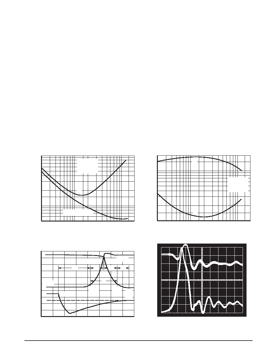
Figure 11. Turn–On Time
IC, COLLECTOR CURRENT (AMP)
tr
td @ VBE(off) = 5 V
100
50
1K
700
500
IC, COLLECTOR CURRENT (AMP)
0.7
3
12
0.2
VCC = 125 V
IC/IB = 5
TJ = 25°C
0.5
200
300
t,TIME
(ns)
0.3
Figure 12. Turn–Off Time
200
100
2K
1K
700
VCC = 125 V
IC/IB = 5
TJ = 25°C
300
500
t,TIME
(ns)
70
7
5
10
20
0.7
1
2
0.2
0.5
0.3
7
510
20
ts
tf
Figure 13. Inductive Switching Measurements
TIME
Figure 14. Typical Inductive Switching Waveforms
(at 300 V and 12 A with IB1 = 2.4 A and VBE(off) = 5 V)
TIME 20 ns/DIV
IC
VCE
IC
VCE
CURRENT
2
A/DIV
VOL
TAGE
50
V/DIV
IC
Vclamp
IB
90% IB1
10%
VCEM
10%
ICM
2%
IC
Vclamp
90% VCEM
90% IC
tsv
trv
tfi
tti
tc
RESISTIVE SWITCHING PERFORMANCE
相关PDF资料 |
PDF描述 |
|---|---|
| MJE13009BG | 12 A, 400 V, NPN, Si, POWER TRANSISTOR |
| MJE1320DW | 2 A, 900 V, NPN, Si, POWER TRANSISTOR |
| MJE1320BV | 2 A, 900 V, NPN, Si, POWER TRANSISTOR |
| MJE1320BA | 2 A, 900 V, NPN, Si, POWER TRANSISTOR |
| MJE1320AN | 2 A, 900 V, NPN, Si, POWER TRANSISTOR |
相关代理商/技术参数 |
参数描述 |
|---|---|
| MJE13009D | 制造商:UTC-IC 制造商全称:UTC-IC 功能描述:HIGH VOLTAGE FAST-SWITCHING NPN POWER TRANSISTOR |
| MJE13009DG-TA3-T | 制造商:UTC-IC 制造商全称:UTC-IC 功能描述:HIGH VOLTAGE FAST-SWITCHING NPN POWER TRANSISTOR |
| MJE13009DL-TA3-T | 制造商:UTC-IC 制造商全称:UTC-IC 功能描述:HIGH VOLTAGE FAST-SWITCHING NPN POWER TRANSISTOR |
| MJE13009F | 制造商:KEC 制造商全称:KEC(Korea Electronics) 功能描述:TRIPLE DIFFUSED NPN TRANSISTOR |
| MJE13009G | 功能描述:两极晶体管 - BJT 12A 400V 100W NPN RoHS:否 制造商:STMicroelectronics 配置: 晶体管极性:PNP 集电极—基极电压 VCBO: 集电极—发射极最大电压 VCEO:- 40 V 发射极 - 基极电压 VEBO:- 6 V 集电极—射极饱和电压: 最大直流电集电极电流: 增益带宽产品fT: 直流集电极/Base Gain hfe Min:100 A 最大工作温度: 安装风格:SMD/SMT 封装 / 箱体:PowerFLAT 2 x 2 |
发布紧急采购,3分钟左右您将得到回复。