- 您现在的位置:买卖IC网 > PDF目录69035 > MM908E630CVFC (FREESCALE SEMICONDUCTOR INC) MICROCONTROLLER, QCC44 PDF资料下载
参数资料
| 型号: | MM908E630CVFC |
| 厂商: | FREESCALE SEMICONDUCTOR INC |
| 元件分类: | 微控制器/微处理器 |
| 英文描述: | MICROCONTROLLER, QCC44 |
| 封装: | 9 X 9 MM, 1 MM HEIGHT, 0.65 MM PITCH, ROHS COMPLIANT, QFN-44 |
| 文件页数: | 21/48页 |
| 文件大小: | 2299K |
| 代理商: | MM908E630CVFC |
第1页第2页第3页第4页第5页第6页第7页第8页第9页第10页第11页第12页第13页第14页第15页第16页第17页第18页第19页第20页当前第21页第22页第23页第24页第25页第26页第27页第28页第29页第30页第31页第32页第33页第34页第35页第36页第37页第38页第39页第40页第41页第42页第43页第44页第45页第46页第47页第48页
Analog Integrated Circuit Device Data
28
Freescale Semiconductor
908E630
FUNCTIONAL DEVICE OPERATION
OPERATIONAL MODES
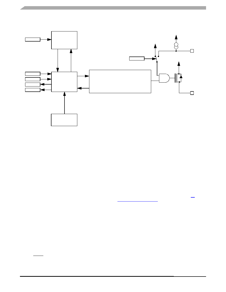
Figure 14. High Side Drivers HS1 and HS2
Open load detection
Each high side driver signals an open load condition if the
current through the high side is below the open load current
threshold.
The open load condition is indicated with the bits HS1OP
and HS2OP in the High Side Status Register.
Current Limitation
Each high side driver has a current limitation limiting the
output current. In combination with the over-temperature
shutdown, the high side drivers are protected against over-
current and short-circuit failures.
The driver operates in the current limitation area and is
indicated with the bits HS1CL and HS2CL in the High Side
Status Register.
Note: If the drivers is operating in current limitation mode
excessive power might be dissipated.
Over-temperature Protection (HS Interrupt)
Both high side drivers are protected against over-
temperature. In case of an over-temperature condition, both
high side drivers are shut down and the event is latched in the
Interrupt Control Module. The shutdown is indicated as an HS
Interrupt in the Interrupt Source Register.
A thermal shutdown of the high side drivers is indicated by
setting all HSxOP and HSxCL bits simultaneously.
If the bit HSM is set in the Interrupt Mask Register than an
Interrupt IRQ_A is generated.
A write to the High Side Control Register, when the over-
temperature condition is gone, will re-enable the high side
drivers.
High Voltage Shutdown
In case of a high voltage condition, and if the high voltage
shutdown is enabled (bit HVSE in the Mode Control Register
is set), both high side drivers are shut down.
A write to the High Side Control Register, when the high
voltage condition is gone, will re-enable the high side drivers.
Sleep and Stop Mode
The high side drivers can be enabled to operate in Sleep
and Stop mode for cyclic sensing. Also see Table 6,
LOW SIDE OUTPUT PINS LS1 AND LS2
These outputs are two low side drivers intended to drive
relays incorporating the following features:
PWM capability up to 10 kHz (software maskable)
open load detection
current limitation
over-temperature shutdown (with maskable interrupt)
active clamp (for driving relays)
high voltage shutdown (software maskable)
The low side switches are controlled by the bit LS1:2 in the
Low Side Control Register.
To protect the device against over-voltage when an
inductive load (relay) is turned off, an active clamp will re-
VS2
VDD
PWMIN
HS1
PWMHS1
HVSE
MOD1:2
HS1
HS1OP
HS1CL
High-voltage
Shutdown
High Side
Interrupt
Cyclic
Sense
on/off
Status
Interrupt
Control
Module
Wake-up
Module
Control
High Side Driver
Charge Pump
Open Load Detection
Over-temperature (interrupt maskable)
High-voltage Shutdown (maskable)
相关PDF资料 |
PDF描述 |
|---|---|
| MN101CP66DBF | 8-BIT, FLASH, 20 MHz, MICROCONTROLLER, PQFP84 |
| MN101CF66DBF | 8-BIT, FLASH, 20 MHz, MICROCONTROLLER, PQFP84 |
| MN101CF66DAL | 8-BIT, FLASH, 20 MHz, MICROCONTROLLER, PQFP80 |
| MN101CP66DAL | 8-BIT, OTPROM, 20 MHz, MICROCONTROLLER, PQFP80 |
| MN103SA7D | 32-BIT, MROM, MICROCONTROLLER, PQFP80 |
相关代理商/技术参数 |
参数描述 |
|---|---|
| MM-90N | 功能描述:ANT MAGN MNT VEHIC 3.5"DIA 10'NF RoHS:是 类别:RF/IF 和 RFID >> RF 天线 系列:* 标准包装:1 系列:* |
| MM90R9F | 制造商:Ohmite Mfg Co 功能描述: |
| MM912_634 | 制造商:FREESCALE 制造商全称:Freescale Semiconductor, Inc 功能描述:Integrated S12 Based Relay Driver with LIN |
| MM912_634_12 | 制造商:FREESCALE 制造商全称:Freescale Semiconductor, Inc 功能描述:Integrated S12 Based Relay Driver with LIN |
| MM912_637 | 制造商:FREESCALE 制造商全称:Freescale Semiconductor, Inc 功能描述:Xtrinsic Battery Sensor with LIN for 12 V Lead-acid |
发布紧急采购,3分钟左右您将得到回复。