- 您现在的位置:买卖IC网 > PDF目录69035 > MM908E630CVFC (FREESCALE SEMICONDUCTOR INC) MICROCONTROLLER, QCC44 PDF资料下载
参数资料
| 型号: | MM908E630CVFC |
| 厂商: | FREESCALE SEMICONDUCTOR INC |
| 元件分类: | 微控制器/微处理器 |
| 英文描述: | MICROCONTROLLER, QCC44 |
| 封装: | 9 X 9 MM, 1 MM HEIGHT, 0.65 MM PITCH, ROHS COMPLIANT, QFN-44 |
| 文件页数: | 22/48页 |
| 文件大小: | 2299K |
| 代理商: | MM908E630CVFC |
第1页第2页第3页第4页第5页第6页第7页第8页第9页第10页第11页第12页第13页第14页第15页第16页第17页第18页第19页第20页第21页当前第22页第23页第24页第25页第26页第27页第28页第29页第30页第31页第32页第33页第34页第35页第36页第37页第38页第39页第40页第41页第42页第43页第44页第45页第46页第47页第48页
Analog Integrated Circuit Device Data
Freescale Semiconductor
29
908E630
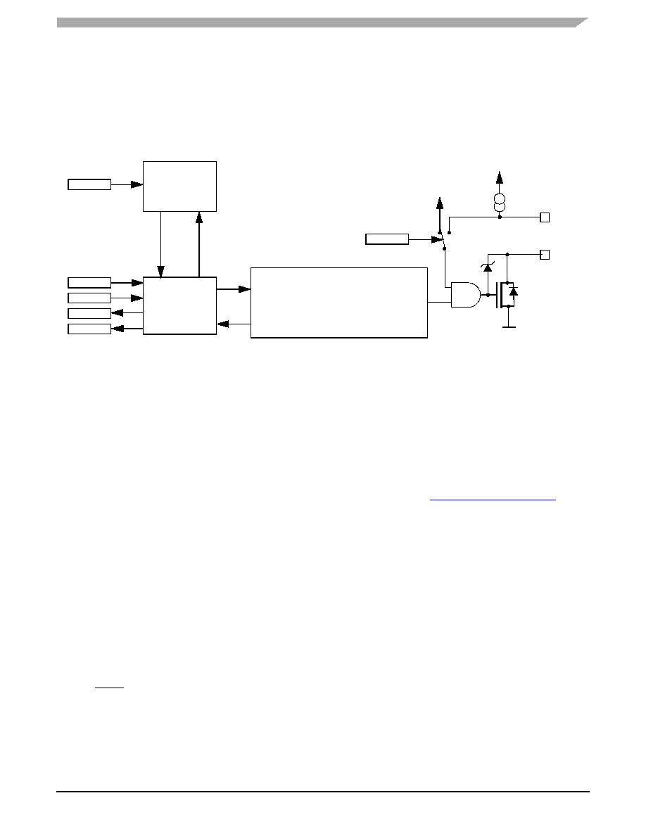
FUNCTIONAL DEVICE OPERATION
OPERATIONAL MODES
enable the low side FET if the voltage on the LS1 or LS2 pin
exceeds a certain level.
PWM capability (direct access)
Each low side driver offers additional (to the SPI control)
direct control via the PWMIN pin.
If both the bits LS1 and PWMLS1 are set in the Low Side
Control Register, then the LS1 driver is turned on if the
PWMIN pin is high and turned off if the PWMIN pin is low. The
same applies to the LS2 and PWMLS2 bits for the LS2 driver.
Figure 15. Low Side Drivers LS1 and LS2
Open Load Detection
Each low side driver signals an open load condition if the
current through the low side is below the open load current
threshold.
The open load condition is indicated with the bit LS1OP
and LS2OP in the Low Side Status Register.
Current Limitation
Each low side driver has a current limitation limiting the
output current. In combination with the over-temperature
shutdown, the low side drivers are protected against over-
current and short-circuit failures.
The driver operates in the current limitation area and is
indicated with the bits LS1CL and LS2CL in the Low Side
Status Register.
Note: If the drivers is operating in current limitation mode
excessive power might be dissipated.
Over-temperature Protection (LS Interrupt)
Both low side drivers are protected against over-
temperature. In case of an over-temperature condition, both
low side drivers are shut down and the event is latched in the
Interrupt Control Module. The shutdown is indicated as LS
Interrupt in the Interrupt Source Register.
If the bit LSM is set in the Interrupt Mask Register than an
Interrupt IRQ_A is generated.
A write to the Low Side Control Register, when the over-
temperature condition is gone, will re-enable the Low Side
Drivers.
High voltage shutdown
In case of an high voltage condition and if the high voltage
shutdown is enabled (bit HVSE in the Mode Control Register
is set) both Low Side drivers are shut down.
A write to the Low Side Control Register, when the high
voltage condition is gone, will re-enable the Low Side Drivers.
Sleep and Stop Mode
The Low Side drivers are disabled in Sleep and Stop
mode. Also see Table 6, Operating Modes Overview.
LIN PHYSICAL LAYER
The LIN bus pin provides a physical layer for single-wire
communication in automotive applications. The LIN physical
layer is designed to meet the LIN physical layer specification
and has the following features:
LIN physical layer 2.0, 2.1, and SAEJ2602 compliant
Slew rate Selection
Over-temperature Shutdown
Advanced Diagnostics
LIN Dominant Voltage Level Selection
The LIN driver is a low side MOSFET with over-current
and thermal shutdown. An internal pull-up resistor with a
serial diode structure is integrated, so no external pull-up
components are required for the application in a slave node.
The fall time from dominant to recessive and the rise time
from recessive to dominant is controlled. The symmetry
between both slopes is guaranteed.
VDD
PWMIN
PGND
PWMHS1
HVSE
MOD1:2
LSx
LSxOP
LSxCL
High-voltage
Shutdown
High Side
Interrupt
on/off
Status
Interrupt
Control
Module
Control
LS Driver
(Active Clamp)
Open Load Detection
Over-temperature (interrupt maskable)
High-voltage Shutdown (maskable)
LSx
Current Limitation
Active
Clamp
相关PDF资料 |
PDF描述 |
|---|---|
| MN101CP66DBF | 8-BIT, FLASH, 20 MHz, MICROCONTROLLER, PQFP84 |
| MN101CF66DBF | 8-BIT, FLASH, 20 MHz, MICROCONTROLLER, PQFP84 |
| MN101CF66DAL | 8-BIT, FLASH, 20 MHz, MICROCONTROLLER, PQFP80 |
| MN101CP66DAL | 8-BIT, OTPROM, 20 MHz, MICROCONTROLLER, PQFP80 |
| MN103SA7D | 32-BIT, MROM, MICROCONTROLLER, PQFP80 |
相关代理商/技术参数 |
参数描述 |
|---|---|
| MM-90N | 功能描述:ANT MAGN MNT VEHIC 3.5"DIA 10'NF RoHS:是 类别:RF/IF 和 RFID >> RF 天线 系列:* 标准包装:1 系列:* |
| MM90R9F | 制造商:Ohmite Mfg Co 功能描述: |
| MM912_634 | 制造商:FREESCALE 制造商全称:Freescale Semiconductor, Inc 功能描述:Integrated S12 Based Relay Driver with LIN |
| MM912_634_12 | 制造商:FREESCALE 制造商全称:Freescale Semiconductor, Inc 功能描述:Integrated S12 Based Relay Driver with LIN |
| MM912_637 | 制造商:FREESCALE 制造商全称:Freescale Semiconductor, Inc 功能描述:Xtrinsic Battery Sensor with LIN for 12 V Lead-acid |
发布紧急采购,3分钟左右您将得到回复。