- 您现在的位置:买卖IC网 > PDF目录385639 > MT46V2M32V1 (Micron Technology, Inc.) DOUBLE DATA RATE DDR SDRAM PDF资料下载
参数资料
| 型号: | MT46V2M32V1 |
| 厂商: | Micron Technology, Inc. |
| 英文描述: | DOUBLE DATA RATE DDR SDRAM |
| 中文描述: | 双倍数据速率的DDR SDRAM内存 |
| 文件页数: | 47/65页 |
| 文件大小: | 2360K |
| 代理商: | MT46V2M32V1 |
第1页第2页第3页第4页第5页第6页第7页第8页第9页第10页第11页第12页第13页第14页第15页第16页第17页第18页第19页第20页第21页第22页第23页第24页第25页第26页第27页第28页第29页第30页第31页第32页第33页第34页第35页第36页第37页第38页第39页第40页第41页第42页第43页第44页第45页第46页当前第47页第48页第49页第50页第51页第52页第53页第54页第55页第56页第57页第58页第59页第60页第61页第62页第63页第64页第65页
47
64Mb: x32 DDR SDRAM
2M32DDR-07.p65
–
Rev. 12/01
Micron Technology, Inc., reserves the right to change products or specifications without notice.
2001, Micron Technology, Inc.
64Mb: x32
DDR SDRAM
4.
AC timing and I
DD
tests may use a V
IL
-to-V
IH
swing
of up to 1.5V in the test environment, but input
timing is still referenced to V
REF
(or to the crossing
point for CK/CK#), and parameter specifications
are guaranteed for the specified AC input levels
under normal use conditions. The minimum slew
rate for the input signals used to test the device is
1V/ns in the range between V
IL
(
AC
) and V
IH
(
AC
).
The AC and DC input level specifications are as
defined in the SSTL_2 Standard (i.e., the receiver
will effectively switch as a result of the signal
crossing the AC input level, and will remain in
that state as long as the signal does not ring back
above [below] the DC input LOW [HIGH] level).
V
REF
is expected to equal V
DD
Q/2 of the transmit-
ting device and to track variations in the DC level
of the same. Peak-to-peak noise on V
REF
may not
exceed ±2 percent of the DC value. Thus, from
V
DD
Q/2, V
REF
is allowed ±25mV for DC error and an
additional ±25mV for AC noise.
V
TT
is not applied directly to the device. V
TT
is a
system supply for signal termination resistors, is
expected to be set equal to V
REF
and must track
variations in the DC level of V
REF
.
V
ID
is the magnitude of the difference between
the input level on CK and the input level on CK#.
The value of V
IX
is expected to equal V
DD
Q/2 of
the transmitting device and must track variations
in the DC level of the same.
10. I
DD
is dependent on output loading and cycle
rates. Specified values are obtained with
minimum cycle time at CL = 3. Outputs are open
during IDD measurements.
11. Enables on-chip refresh and address counters.
12. I
DD
specifications are tested after the device is
properly initialized.
5.
6.
7.
8.
9.
NOTES
1.
All voltages referenced to V
SS
.
2.
Tests for AC timing, I
DD
, and electrical AC and DC
characteristics may be conducted at nominal
reference/supply voltage levels, but the related
specifications and device operation are guaran-
teed for the full voltage range specified.
3.
Outputs measured with equivalent load:
13. This parameter is sampled. V
DD
= +2.5V/+2.65V
+0.1V/-0.1V, V
DD
Q = +2.5V/+2.65V +0.1V -0.1, V
REF
= V
SS
, f = 100 MHz, T
A
= 25°C, V
OUT
(
DC
) = V
DD
Q/2,
V
OUT
(peak to peak) = 0.2V. DM input is grouped
with I/O pins, reflecting the fact that they are
matched in loading.
14. Command/Address input slew rate = 0.5V/ns. For
slew rates 1V/ns or faster,tIS and tIH are reduced
to 900ps. If the slew rate is less than 0.5V/ns,
timing must be derated:tIS has an additional
100ps per 100mV/ns reduction in slew rate from
500mV/ns. If the slew rate exceeds 4.5V/ns,
functionality is uncertain.
15. The CK/CK# input reference level (for timing
referenced to CK/CK#) is the point at which CK
and CK# cross; the input reference level for
signals other than CK/CK# is V
REF
.
16. Inputs are not recognized as valid until V
REF
stabilizes. Exception: during the period before
V
REF
stabilizes, CKE
≤
0.3 x V
DD
Q is recognized as
LOW.
17. The output timing reference level, as measured
at the timing reference point indicated in Note 3,
is V
TT
.
18.
t
HZ and
t
LZ transitions occur in the same access
time windows as valid data transitions. These
parameters are not referenced to a specific
voltage level, but specify when the device output
is no longer driving (HZ) or begins driving (LZ).
19. The maximum limit for this parameter is not a
device limit. The device will operate with a
greater value for this parameter, but system
performance (bus turnaround) will degrade
accordingly.
20. This is not a device limit. The device will operate
with a negative value, but system performance
could be degraded due to bus turnaround.
21. It is recommended that DQS be valid (HIGH or
LOW) on or before the WRITE command. The
case shown (DQS going from High-Z to logic LOW)
applies when no WRITEs were previously in
progress on the bus. If a previous WRITE was in
progress, DQS could be HIGH during this time,
depending on
t
DQSS.
22. MIN (
t
RC or
t
RFC) for I
DD
measurements is the
smallest multiple of
t
CK that meets the minimum
absolute value for the respective parameter.
t
RAS (MAX) for I
DD
measurements is the largest
multiple of
t
CK that meets the maximum
absolute value for
t
RAS.
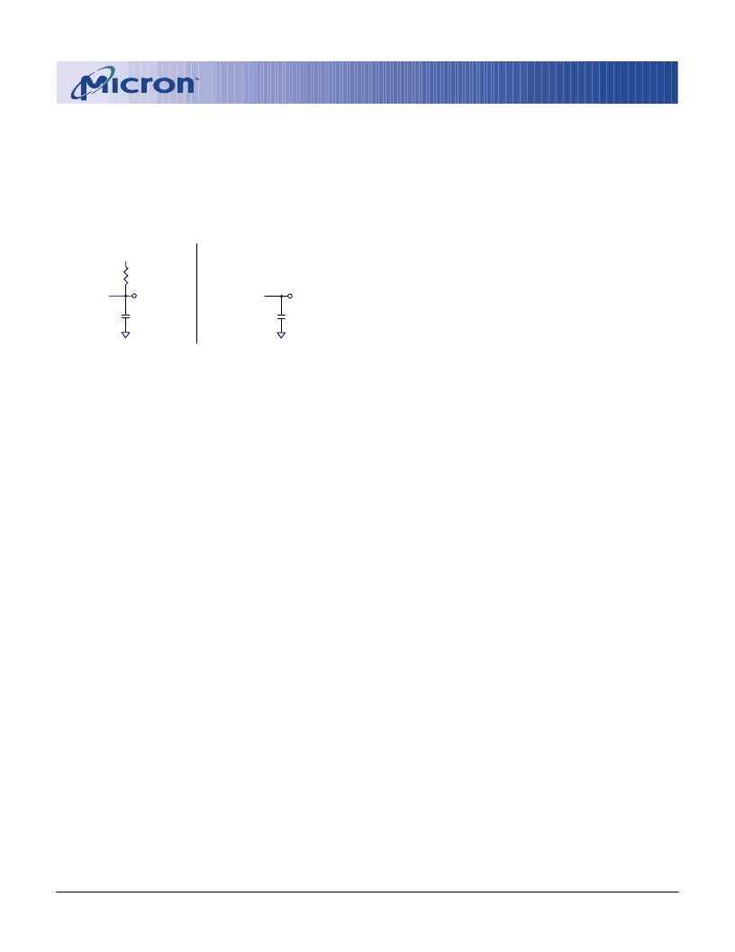
Output
(V
OUT
)
,
Reduced
Drive)
Reference
Point
20pF
50
V
TT
Output
(V
OUT
)
,
Impedance
Match
Reference
Point
20pF
相关PDF资料 |
PDF描述 |
|---|---|
| MT46V32M4-1 | DOUBLE DATA RATE DDR SDRAM |
| MT46V32M4TG-75 | DOUBLE DATA RATE DDR SDRAM |
| MT46V32M4TG-75L | DOUBLE DATA RATE DDR SDRAM |
| MT46V32M4TG-75Z | DOUBLE DATA RATE DDR SDRAM |
| MT46V32M4TG-75ZL | DOUBLE DATA RATE DDR SDRAM |
相关代理商/技术参数 |
参数描述 |
|---|---|
| MT46V32M16 | 制造商:Micron Technology Inc 功能描述:32MX16 DDR SDRAM PLASTIC IND TEMP BGA 2.6V DDR - Trays |
| MT46V32M16-5B | 制造商:Micron Technology Inc 功能描述: |
发布紧急采购,3分钟左右您将得到回复。