- 您现在的位置:买卖IC网 > PDF目录385639 > MT46V2M32V1 (Micron Technology, Inc.) DOUBLE DATA RATE DDR SDRAM PDF资料下载
参数资料
| 型号: | MT46V2M32V1 |
| 厂商: | Micron Technology, Inc. |
| 英文描述: | DOUBLE DATA RATE DDR SDRAM |
| 中文描述: | 双倍数据速率的DDR SDRAM内存 |
| 文件页数: | 48/65页 |
| 文件大小: | 2360K |
| 代理商: | MT46V2M32V1 |
第1页第2页第3页第4页第5页第6页第7页第8页第9页第10页第11页第12页第13页第14页第15页第16页第17页第18页第19页第20页第21页第22页第23页第24页第25页第26页第27页第28页第29页第30页第31页第32页第33页第34页第35页第36页第37页第38页第39页第40页第41页第42页第43页第44页第45页第46页第47页当前第48页第49页第50页第51页第52页第53页第54页第55页第56页第57页第58页第59页第60页第61页第62页第63页第64页第65页
48
64Mb: x32 DDR SDRAM
2M32DDR-07.p65
–
Rev. 12/01
Micron Technology, Inc., reserves the right to change products or specifications without notice.
2001, Micron Technology, Inc.
64Mb: x32
DDR SDRAM
23. The refresh period 32ms. This equates to an
average refresh rate of 7.8μs. However, an AUTO
REFRESH command must be asserted at least
once every 70.2μs; burst refreshing or posting by
the DRAM controller greater than eight refresh
cycles is not allowed.
24. The I/O capacitance per DQS and DQ byte/group
will not differ by more than this maximum
amount for any given device.
25. The valid data window is derived by achieving
other specifications —
t
HP (
t
CK/2),
t
DQSQ, and
t
QH [
t
HP - 0.5ns (-5),
t
HP - 0.55ns (-55)
,t
HP - 0.6ns
(-6) or
t
HP - 0.65ns (-65)]. The data valid window
derates directly porportional with the clock duty
cycle and a practical data valid window can be
derived. The clock is allowed a maximum duty
cycle variation of 45/55. Functionality is uncer-
tain when operating beyond a 45/55 ratio. The
data valid window derating curves are provided
below for duty cycles ranging between 50/50 and
45/55.
26. Referenced to each output group: DQS with DQ0-
DQ31
NOTES (continued)
27. This limit is actually a nominal value and does
not result in a fail value. CKE is HIGH during
REFRESH command period (
t
RFC [MIN]) else
CKE is LOW (i.e., during standby).
28. To maintain a valid level, the transitioning edge
of the input must:
a) Sustain a constant slew rate from the current
AC level through to the target AC level, V
IL
(
AC
)
or V
IH
(
AC
).
b) Reach at least the target AC level.
c) After the AC target level is reached, continue
to maintain at least the target DC level, V
IL
(
DC
)
or V
IH
(
DC
).
29. The Input capacitance per pin group will not
differ by more than this maximum amount for
any given device..
30. CK and CK# input slew rate must be
≥
1V/ns.
31. DQ and DM input slew rates must not deviate
from DQS by more than 10%. If the DQ/DM/DQS
slew rate is less than 0.5V/ns, timing is no longer
referenced to the mid-point but to the V
IL
(
AC
)
maximum and V
IH
(
DC
) minimum points.
32. V
DD
must not vary more than 4% if CKE is not
active while any bank is active.
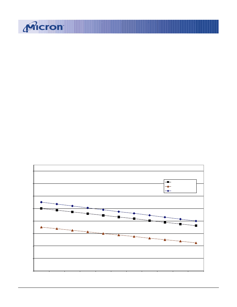
DERATING DATA VALID WINDOW
(
t
QH -
t
DQSQ) at CL = 3
1.525
1.553
1.580
1.608
1.635
1.663
1.690
1.718
1.745
1.773
1.800
1.250
1.275
1.300
1.325
1.350
1.375
1.400
1.425
1.450
1.475
1.500
1.600
1.630
1.660
1.690
1.720
1.750
1.780
1.810
1.840
1.870
1.900
0.8
1.0
1.2
1.4
1.6
1.8
2.0
2.2
2.4
1.900
1.870
1.840
1.810
1.780
1.750
1.720
1.690
1.660
1.630
1.600
Clock Duty Cycle
n
-5.5 @ tCK = 5.5ns
-5 @ tCK = 5ns
-6 @ tCK = 6ns
相关PDF资料 |
PDF描述 |
|---|---|
| MT46V32M4-1 | DOUBLE DATA RATE DDR SDRAM |
| MT46V32M4TG-75 | DOUBLE DATA RATE DDR SDRAM |
| MT46V32M4TG-75L | DOUBLE DATA RATE DDR SDRAM |
| MT46V32M4TG-75Z | DOUBLE DATA RATE DDR SDRAM |
| MT46V32M4TG-75ZL | DOUBLE DATA RATE DDR SDRAM |
相关代理商/技术参数 |
参数描述 |
|---|---|
| MT46V32M16 | 制造商:Micron Technology Inc 功能描述:32MX16 DDR SDRAM PLASTIC IND TEMP BGA 2.6V DDR - Trays |
| MT46V32M16-5B | 制造商:Micron Technology Inc 功能描述: |
发布紧急采购,3分钟左右您将得到回复。