- 您现在的位置:买卖IC网 > PDF目录299522 > MT58L128V18PF-6 (CYPRESS SEMICONDUCTOR CORP) 128K X 18 STANDARD SRAM, 3.5 ns, PBGA165 PDF资料下载
参数资料
| 型号: | MT58L128V18PF-6 |
| 厂商: | CYPRESS SEMICONDUCTOR CORP |
| 元件分类: | SRAM |
| 英文描述: | 128K X 18 STANDARD SRAM, 3.5 ns, PBGA165 |
| 封装: | FBGA-165 |
| 文件页数: | 24/25页 |
| 文件大小: | 647K |
| 代理商: | MT58L128V18PF-6 |
8
2Mb: 128K x 18, 64K x 32/36 Pipelined, SCD SyncBurst SRAM
Micron Technology, Inc., reserves the right to change products or specifications without notice.
MT58L128L18P_2.p65 – Rev. 8/00
2000, Micron Technology, Inc.
2Mb: 128K x 18, 64K x 32/36
PIPELINED, SCD SYNCBURST SRAM
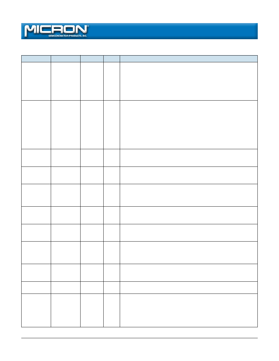
FBGA PIN DESCRIPTIONS
x18
x32/x36
SYMBOL
TYPE
DESCRIPTION
6R
SA0
Input
Synchronous Address Inputs: These inputs are registered and must
6P
SA1
meet the setup and hold times around the rising edge of CLK.
2A, 2B, 3P,
SA
3R, 4P, 4R,
8P, 8R, 9P,
9R, 10A, 10B 9R, 10A, 10B
10P, 10R, 11A
10P, 10R
5B
BWa#
Input
Synchronous Byte Write Enables: These active LOW inputs allow
4A
5A
BWb#
individual bytes to be written and must meet the setup and hold
–
4A
BWc#
times around the rising edge of CLK. A byte write enable is LOW
–
4B
BWd#
for a WRITE cycle and HIGH for a READ cycle. For the x18 version,
BWa# controls DQas and DQPa; BWb# controls DQbs and DQPb. For
the x32 and x36 versions, BWa# controls DQas and DQPa; BWb#
controls DQbs and DQPb; BWc# controls DQcs and DQPc; BWd#
controls DQds and DQPd. Parity is only available on the x18 and x36
versions.
7A
BWE#
Input
Byte Write Enable: This active LOW input permits BYTE WRITE
operations and must meet the setup and hold times around the
rising edge of CLK.
7B
GW#
Input
Global Write: This active LOW input allows a full 18-, 32-, or 36-bit
WRITE to occur independent of the BWE# and BWx# lines and must
meet the setup and hold times around the rising edge of CLK.
6B
CLK
Input
Clock: This signal registers the address, data, chip enable, byte write
enables, and burst control inputs on its rising edge. All synchronous
inputs must meet setup and hold times around the clock’s rising
edge.
3A
CE#
Input
Synchronous Chip Enable: This active LOW input is used to enable
the device and conditions the internal use of ADSP#. CE# is sampled
only when a new external address is loaded.
6A
CE2#
Input
Synchronous Chip Enable: This active LOW input is used to enable
the device and is sampled only when a new external address is
loaded.
11H
ZZ
Input
Snooze Enable: This active HIGH, asynchronous input causes the
device to enter a low-power standby mode in which all data in the
memory array is retained. When ZZ is active, all other inputs are
ignored.
3B
CE2
Input
Synchronous Chip Enable: This active HIGH input is used to enable
the device and is sampled only when a new external address is
loaded.
8B
OE#(G#)
Input
Output Enable: This active LOW, asynchronous input enables the
data I/O output drivers.
9A
ADV#
Input
Synchronous Address Advance: This active LOW input is used to
advance the internal burst counter, controlling burst access after the
external address is loaded. A HIGH on ADV# effectively causes wait
states to be generated (no address advance). To ensure use of
correct address during a WRITE cycle, ADV# must be HIGH at the
rising edge of the first clock after an ADSP# cycle is initiated.
(continued)
相关PDF资料 |
PDF描述 |
|---|---|
| MT58L64V36PF-10 | 64K X 36 STANDARD SRAM, 5 ns, PBGA165 |
| MT58L256L36FS-8.8 | 256K X 36 STANDARD SRAM, 7.5 ns, PQFP100 |
| MT58LC64K16E1S27BDC1 | 64K X 16 STANDARD SRAM, UUC75 |
| MT58LC64K16E1S27BDC3-8.5 | 64K X 16 STANDARD SRAM, 8.5 ns, UUC75 |
| MT58LC64K32C4LG-5L | 64K X 32 STANDARD SRAM, PQFP100 |
相关代理商/技术参数 |
参数描述 |
|---|---|
| MT58L128V18PT-7.5 | 制造商:Micron Technology Inc 功能描述: |
| MT58L128V32F1 | 制造商:MICRON 制造商全称:Micron Technology 功能描述:4Mb: 256K x 18, 128K x 32/36 FLOW-THROUGH SYNCBURST SRAM |
| MT58L128V32P1T-10 | 制造商:Rochester Electronics LLC 功能描述:- Bulk 制造商:Micron Technology Inc 功能描述: |
| MT58L128V32P1T-7.5 | 制造商:Rochester Electronics LLC 功能描述:- Bulk |
| MT58L128V36F1 | 制造商:MICRON 制造商全称:Micron Technology 功能描述:4Mb: 256K x 18, 128K x 32/36 FLOW-THROUGH SYNCBURST SRAM |
发布紧急采购,3分钟左右您将得到回复。