- 您现在的位置:买卖IC网 > PDF目录299522 > MT58L128V18PF-6 (CYPRESS SEMICONDUCTOR CORP) 128K X 18 STANDARD SRAM, 3.5 ns, PBGA165 PDF资料下载
参数资料
| 型号: | MT58L128V18PF-6 |
| 厂商: | CYPRESS SEMICONDUCTOR CORP |
| 元件分类: | SRAM |
| 英文描述: | 128K X 18 STANDARD SRAM, 3.5 ns, PBGA165 |
| 封装: | FBGA-165 |
| 文件页数: | 7/25页 |
| 文件大小: | 647K |
| 代理商: | MT58L128V18PF-6 |
15
2Mb: 128K x 18, 64K x 32/36 Pipelined, SCD SyncBurst SRAM
Micron Technology, Inc., reserves the right to change products or specifications without notice.
MT58L128L18P_2.p65 – Rev. 8/00
2000, Micron Technology, Inc.
2Mb: 128K x 18, 64K x 32/36
PIPELINED, SCD SYNCBURST SRAM
NOTE: 1. VDDQ = +3.3V +0.3V/-0.165V for 3.3V I/O configuration; VDDQ = +2.5V +0.4V/-0.125V for 2.5V I/O configuration.
2. IDD is specified with no output current and increases with faster cycle times. IDDQ increases with faster cycle times
and greater output loading.
3. “Device deselected” means device is in power-down mode as defined in the truth table. “Device selected” means device
is active (not in power-down mode).
4. Typical values are measured at 3.3V, 25°C and 10ns cycle time.
5. This parameter is sampled.
6. Preliminary package data.
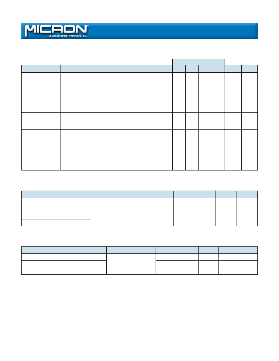
TQFP CAPACITANCE
DESCRIPTION
CONDITIONS
SYMBOL
TYP
MAX
UNITS
NOTES
Control Input Capacitance
TA = 25°C; f = 1 MHz;
CI
2.7
3.5
p F
5
Input/Output Capacitance (DQ)
VDD = 3.3V
CO
45
p F
5
Address Capacitance
CA
2.5
3.5
p F
5
Clock Capacitance
CCK
2.5
3.5
p F
5
IDD OPERATING CONDITIONS AND MAXIMUM LIMITS
(Note 1) (0°C
≤ T
A ≤ +70°C; VDD = +3.3V +0.3V/-0.165V unless otherwise noted)
DESCRIPTION
CONDITIONS
SYM
TYP
-5
-6
-7.5
-10
UNITS NOTES
Power Supply
Device selected; All inputs
≤ VIL
Current:
or
≥ VIH; Cycle time ≥ tKC (MIN);
IDD
100
400
340
280
225
mA
2, 3, 4
Operating
VDD = MAX; Outputs open
Power Supply
Device selected; VDD = MAX;
Current: Idle
ADSC#, ADSP#, GW#, BWx#, ADV#
≥
IDD1
30
100
85
70
65
mA
2, 3, 4
VIH; All inputs
≤ VSS + 0.2 or ≥ VDD - 0.2;
Cycle time
≥ tKC (MIN)
CMOS Standby
Device deselected; VDD = MAX;
All inputs
≤ VSS + 0.2 or ≥ VDD - 0.2;
ISB2
0.5
10
mA
3, 4
All inputs static; CLK frequency = 0
TTL Standby
Device deselected; VDD = MAX;
All inputs
≤ VIL or ≥ VIH;ISB3
6
25252525
mA
3, 4
All inputs static; CLK frequency = 0
Clock Running
Device deselected; VDD = MAX;
ADSC#, ADSP#, GW#, BWx#, ADV#
≥
ISB4
30
100
85
70
65
mA
3, 4
VIH; All inputs
≤ VSS + 0.2 or ≥ VDD - 0.2;
Cycle time
≥ tKC (MIN)
MAX
FBGA CAPACITANCE
DESCRIPTION
CONDITIONS
SYMBOL
TYP
MAX
UNITS
NOTES
Address/Control Input Capacitance
CI
2.5
3.5
p F
5, 6
Output Capacitance (Q)
T
A = 25°C; f = 1 MHz
CO
4
5
p F
5, 6
Clock Capacitance
CCK
2.5
3.5
p F
5, 6
相关PDF资料 |
PDF描述 |
|---|---|
| MT58L64V36PF-10 | 64K X 36 STANDARD SRAM, 5 ns, PBGA165 |
| MT58L256L36FS-8.8 | 256K X 36 STANDARD SRAM, 7.5 ns, PQFP100 |
| MT58LC64K16E1S27BDC1 | 64K X 16 STANDARD SRAM, UUC75 |
| MT58LC64K16E1S27BDC3-8.5 | 64K X 16 STANDARD SRAM, 8.5 ns, UUC75 |
| MT58LC64K32C4LG-5L | 64K X 32 STANDARD SRAM, PQFP100 |
相关代理商/技术参数 |
参数描述 |
|---|---|
| MT58L128V18PT-7.5 | 制造商:Micron Technology Inc 功能描述: |
| MT58L128V32F1 | 制造商:MICRON 制造商全称:Micron Technology 功能描述:4Mb: 256K x 18, 128K x 32/36 FLOW-THROUGH SYNCBURST SRAM |
| MT58L128V32P1T-10 | 制造商:Rochester Electronics LLC 功能描述:- Bulk 制造商:Micron Technology Inc 功能描述: |
| MT58L128V32P1T-7.5 | 制造商:Rochester Electronics LLC 功能描述:- Bulk |
| MT58L128V36F1 | 制造商:MICRON 制造商全称:Micron Technology 功能描述:4Mb: 256K x 18, 128K x 32/36 FLOW-THROUGH SYNCBURST SRAM |
发布紧急采购,3分钟左右您将得到回复。