- 您现在的位置:买卖IC网 > PDF目录224506 > MT58L128V36P1B-4 128K X 36 STANDARD SRAM, 2.3 ns, PBGA119 PDF资料下载
参数资料
| 型号: | MT58L128V36P1B-4 |
| 元件分类: | SRAM |
| 英文描述: | 128K X 36 STANDARD SRAM, 2.3 ns, PBGA119 |
| 封装: | 14 X 22 MM, PLASTIC, MS-028BHA, BGA-119 |
| 文件页数: | 33/35页 |
| 文件大小: | 353K |
| 代理商: | MT58L128V36P1B-4 |
第1页第2页第3页第4页第5页第6页第7页第8页第9页第10页第11页第12页第13页第14页第15页第16页第17页第18页第19页第20页第21页第22页第23页第24页第25页第26页第27页第28页第29页第30页第31页第32页当前第33页第34页第35页
7
4Mb: 256K x 18, 128K x 32/36 Pipelined, SCD SyncBurst SRAM
Micron Technology, Inc., reserves the right to change products or specifications without notice.
MT58L256L18P1_D.p65 – Rev. 10/01
2001, Micron Technology, Inc.
4Mb: 256K x 18, 128K x 32/36
PIPELINED, SCD SYNCBURST SRAM
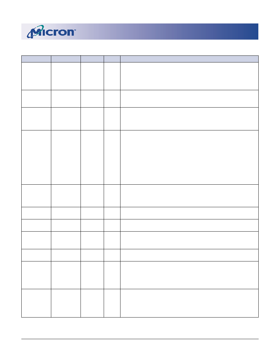
TQFP PIN DESCRIPTIONS (continued)
x18
x32/x36
SYMBOL
TYPE
DESCRIPTION
85
ADSC#
Input
Synchronous Address Status Controller: This active LOW input
interrupts any ongoing burst, causing a new external address to be
registered. A READ or WRITE is performed using the new address if
CE# is LOW. ADSC# is also used to place the chip into power-down
state when CE# is HIGH.
31
MODE
Input
Mode: This input selects the burst sequence. A LOW on this pin
selects “linear burst.” NC or HIGH on this pin selects “interleaved
burst.” Do not alter input state while device is operating.
64
ZZ
Input
Snooze Enable: This active HIGH, asynchronous input causes the
device to enter a low-power standby mode in which all data in the
memory array is retained. When ZZ is active, all other inputs are
ignored.
(a) 58, 59,
(a) 52, 53,
DQa
Input/ SRAM Data I/Os: For the x18 version, Byte “a” is DQa pins; Byte “b”
62, 63, 68, 69, 56-59, 62, 63
Output is DQb pins. For the x32 and x36 versions, Byte “a” is DQa pins;
72, 73
Byte “b” is DQb pins; Byte “c” is DQc pins; Byte “d” is DQd pins.
(b) 8, 9, 12,
(b) 68, 69
DQb
Input data must meet setup and hold times around the rising edge
13, 18, 19, 22, 72-75, 78, 79
of CLK.
23
(c) 2, 3, 6-9,
DQc
12, 13
(d) 18, 19,
DQd
22-25, 28, 29
74
51
NC/DQPa
NC/
No Connect/Parity Data I/Os: On the x32 version, these pins are No
24
80
NC/DQPb
I/O
Connect (NC). On the x18 version, Byte “a” parity is DQPa; Byte “b”
–
1
NC/DQPc
parity is DQPb. On the x36 version, Byte “a” parity is DQPa; Byte
–
30
NC/DQPd
“b” parity is DQPb; Byte “c” parity is DQPc; Byte “d” parity is DQPd.
14, 15, 41, 65, 14, 15, 41, 65,
VDD
Supply Power Supply: See DC Electrical Characteristics and Operating
91
Conditions for range.
4, 11, 20, 27,
VDDQ
Supply Isolated Output Buffer Supply: See DC Electrical Characteristics and
54, 61, 70, 77 54, 61, 70, 77
Operating Conditions for range.
5, 10, 17, 21,
VSS
Supply Ground: GND.
26, 40, 55, 60, 26, 40, 55, 60,
67, 71, 76, 90 67, 71, 76, 90
38, 39
DNU
–
Do Not Use: These signals may either be unconnected or wired to
GND to improve package heat dissipation.
1-3, 6, 7, 16,
16, 66
NC
–
No Connect: These signals are not internally connected and may be
25, 28-30,
connected to ground to improve package heat dissipation.
51-53, 56, 57,
66, 75, 78, 79,
95, 96
42, 43
NF
–
No Function: These pins are internally connected to the die and
have the capacitance of input pins. It is allowable to leave these
pins unconnected or driven by signals. Reserved for address
expansion; pin 43 becomes an SA at 8Mb density and pin 42
becomes an SA at 16Mb density.
相关PDF资料 |
PDF描述 |
|---|---|
| MT58L32L36PT-7.5 | 32K X 36 CACHE SRAM, 4.2 ns, PQFP100 |
| MT58L512L18DS-7.5IT | 512K X 18 CACHE SRAM, 4 ns, PQFP100 |
| MT58L512L18DT-10IT | 512K X 18 CACHE SRAM, 5 ns, PQFP100 |
| MT58L512L18PB-6IT | 512K X 18 STANDARD SRAM, 3.5 ns, PBGA119 |
| MT58L512L18PS-7.5IT | 512K X 18 CACHE SRAM, 4 ns, PQFP100 |
相关代理商/技术参数 |
参数描述 |
|---|---|
| MT58L128V36P1F-5 | 制造商:Rochester Electronics LLC 功能描述:- Bulk 制造商:Micron Technology Inc 功能描述: |
| MT58L128V36P1F-6 | 制造商:Rochester Electronics LLC 功能描述:- Bulk 制造商:Micron Technology Inc 功能描述: |
| MT58L128V36P1T-7.5 | 制造商:Rochester Electronics LLC 功能描述:- Bulk 制造商:Micron Technology Inc 功能描述: |
| MT58L1MV18D | 制造商:MICRON 制造商全称:Micron Technology 功能描述:8Mb: 512K x 18, 256K x 32/36 3.3V I/O, PIPELINED, DCD SYNCBURST SRAM |
| MT58L1MY18D | 制造商:MICRON 制造商全称:Micron Technology 功能描述:16Mb SYNCBURST⑩ SRAM |
发布紧急采购,3分钟左右您将得到回复。